
Datasheet


dsPIC30F1010/202X
DS70178C-page 204 Preliminary © 2006 Microchip Technology Inc.
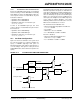
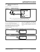
REGISTER 18-6: FOSC: OSCILLATOR SELECTION CONFIGURATION BITS
U-0 U-0 U-0 U-0 U-0 U-0 U-0 U-0
— — — — — — — —
bit 23 bit 16
U-0 U-0 U-0 U-0 U-0 U-0 U-0 U-0
— — — — — — — —
bit 15 bit 8
R/P R/P R/P U-0 U-0 R/P R/P R/P
FCKSM<1:0> FRANGE
— — OSCIOFNC POSCMD<1:0>
bit 7 bit 0
Legend:
R = Readable bit W = Writable bit U = Unimplemented bit, read as ‘0’
-n = Value at POR ‘1’ = Bit is set ‘0’ = Bit is cleared x = Bit is unknown
bit 23-8 Unimplemented: Read as ‘0’
bit 7-6 FCKSM<1:0>: Clock Switching and Monitor Selection Configuration bits
1x = Clock switching is disabled, fail-safe clock monitor is disabled
01 = Clock switching is enabled, fail-safe clock monitor is disabled
00 = Clock switching is enabled, fail-safe clock monitor is enabled
bit 5 FRANGE: Frequency Range Select for FRC and PLL bit
Acts like a “Gear Shift” feature that enables the dsPIC DSC device to operate at reduced MIPS at a
reduced supply voltage (3.3V)
FRANGE
Bit Value
Temperature
Rating
FRC Frequency
(Nominal)
PLL VCO
(Nominal)
1 = High Range Industrial
Extended
14.55 MHz
9.7 MHz
466 MHz (480 MHz max.)
310 MHz (320 MHz max.)
0 = Low Range Industrial
Extended
9.7 MHz
6.4 MHz
310 MHz (320 MHz max.)
205 MHz (211 MHz max.)
bit 4-3 Unimplemented: Read as ‘0’
bit 3 OSCIOFNC: OSC2 Pin I/O Enable bit
1 = CLKO output signal active on the OSCO pin
0 = CLKO output disabled
bit 1-0 POSCMD<1:0>: Primary Oscillator Mode
11 = Primary Oscillator Disabled
10 = HS oscillator mode selected
01 = Reserved
00 = External clock mode selected