
Datasheet


© 2006 Microchip Technology Inc. Preliminary DS70178C-page 197
dsPIC30F1010/202X
18.0 SYSTEM INTEGRATION
There are several features intended to maximize sys-
tem reliability, minimize cost through elimination of
external components, provide power-saving operating
modes and offer code protection:
• Oscillator Selection
• Reset:
- Power-on Reset (POR)
- Power-up Timer (PWRT)
- Oscillator Start-up Timer (OST)
• Watchdog Timer (WDT)
• Power-Saving modes (Sleep and Idle)
• Code Protection
• Unit ID Locations
• In-Circuit Serial Programming (ICSP)
programming capability
dsPIC30F devices have a Watchdog Timer, which can
be permanently enabled via the Configuration bits or
can be software controlled. It runs off its own RC oscil-
lator for added reliability. There are two timers that offer
necessary delays on power-up. One is the Oscillator
Start-up Timer (OST), intended to keep the chip in
Reset until the crystal oscillator is stable. The other is
the Power-up Timer (PWRT), which provides a delay
on power-up only, designed to keep the part in Reset
mode while the power supply stabilizes. With these two
timers on-chip, most applications need no external
Reset circuitry.
Sleep mode is designed to offer a very low-current
Power-Down mode. The user can wake-up from Sleep
mode through external Reset, Watchdog Timer Wake-
up or through an interrupt. Several oscillator options
are also made available to allow the part to fit a wide
variety of applications. In the Idle mode, the clock
sources are still active, but the CPU is shut off. The RC
oscillator option saves system cost, while the LP crystal
option saves power.
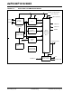
18.1 Oscillator System Overview
The dsPIC30F oscillator system has the following
modules and features:
• Various external and internal oscillator options as
clock sources
• An on-chip PLL to boost internal operating
frequency
• A clock switching mechanism between various
clock sources
• Programmable clock postscaler for system power
savings
• A Fail-Safe Clock Monitor (FSCM) that detects
clock failure and takes fail-safe measures
• Clock Control register OSCCON
• Configuration bits for main oscillator selection
Configuration bits determine the clock source upon
Power-on Reset (POR). Thereafter, the clock source
can be changed between permissible clock sources.
The OSCCON register controls the clock switching and
reflects system clock related status bits.
A simplified diagram of the oscillator system is shown
in Figure 18-1.
18.2 Oscillator Control Registers
The oscillators are controlled with these registers:
• OSCCON: Oscillator Control Register
• OSCTUN2: Oscillator Tuning Register 2
• LFSR: Linear Feedback Shift Register
• FOSCSEL: Oscillator Selection Configuration Bits
• FOSC: Oscillator Selection Configuration Bits
Note: This data sheet summarizes features of this group
of dsPIC30F devices and is not intended to be a complete
reference source. For more information on the CPU,
peripherals, register descriptions and general device
functionality, refer to the “dsPIC30F Family Reference
Manual” (DS70046).
For more information on the device instruction set and pro-
gramming, refer to the “dsPIC30F/33F Programmer’s
Reference Manual” (DS70157).
Note: 32 kHz crystal operation is not enabled on
dsPIC30F1010/202X devices.