
Datasheet


dsPIC30F1010/202X
DS70178C-page 186 Preliminary © 2006 Microchip Technology Inc.
16.17 A/D Sample and Convert Timing
The sample and hold circuits assigned to the input pins
have their own timing logic that is triggered when an
external sample and convert request (from PWM or
TMR) is made. The sample and hold circuits have a
fixed two clock data sample period. When the sample
has been acquired, then the ADC control logic is noti-
fied of a pending request, then the conversion is
performed as the conversion resources become
available.
The ADC module always converts pairs of analog input
channels, so a typical conversion process requires 24
clock cycles.
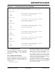
FIGURE 16-3: DETAILED CONVERSION SEQUENCE TIMINGS, SEQSAMP = 0, NOT BUSY
10th 9th 8th 7th 6th 5th 4th 3rd 2nd 1st
TAD
adc_clk
sample_even
convert_en
capture_first_data
10th 9th 8th 7th 6th 5th 4th 3rd 2nd 1st
4 5 6 7 8 9 10 11 12 13 14 15 16 17 18 19 20 21 0 1
2
0 1 2 3
connect_second
connect_first
state counter
capture_second_data
sample_odd