
Datasheet


dsPIC30F1010/202X
DS70178C-page 174 Preliminary © 2006 Microchip Technology Inc.
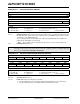
REGISTER 16-3: A/D BASE REGISTER (ADBASE)
R/W-0 R/W-0 R/W-0 R/W-0 R/W-0 R/W-0 R/W-0 R/W-0
ADBASE<15:8>
bit 15 bit 8
R/W-0 R/W-0 R/W-0 R/W-0 R/W-0 R/W-0 R/W-0 U-0
ADBASE<7:1>
—
bit 7 bit 0
Legend:
R = Readable bit W = Writable bit U = Unimplemented bit, read as ‘0’
-n = Value at POR ‘1’ = Bit is set ‘0’ = Bit is cleared x = Bit is unknown
bit 15-1 ADC Base Register: This register contains the base address of the user’s ADC Interrupt Service Rou-
tine jump table. This register, when read, contains the sum of the ADBASE register contents and the
encoded value of the PxRDY Status bits.
The encoder logic provides the bit number of the highest priority PxRDY bits where P0RDY is the
highest priority, and P5RDY is lowest priority.
Note: The encoding results are shifted left two bits so bits 1-0 of the result are always zero.
bit 0 Unimplemented: Read as ‘0’
Note: As an alternative to using the ADBASE Register, the ADCP0-5 ADC Pair Conversion Complete Interrupts
(Interrupts 37-42) can be used to invoke A to D conversion completion routines for individual ADC input
pairs. Refer to Section 16.9 “Individual Pair Interrupts”.
REGISTER 16-4: A/D PORT CONFIGURATION REGISTER (ADPCFG)
U-0 U-0 U-0 U-0 R/W-0 R/W-0 R/W-0 R/W-0
— — — — PCFG11 PCFG10 PCFG9 PCFG8
bit 15 bit 8
R/W-0 R/W-0 R/W-0 R/W-0 R/W-0 R/W-0 R/W-0 R/W-0
PCFG7 PCFG6 PCFG5 PCFG4 PCFG3 PCFG2 PCFG1 PCFG0
bit 7 bit 0
Legend:
R = Readable bit W = Writable bit U = Unimplemented bit, read as ‘0’
-n = Value at POR ‘1’ = Bit is set ‘0’ = Bit is cleared x = Bit is unknown
bit 15-12 Unimplemented: Read as ‘0’
bit 11-0 PCFG<11:0>: A/D Port Configuration Control bits
1 = Port pin in Digital mode, port read input enabled, A/D input multiplexor connected to AV
SS
0 = Port pin in Analog mode, port read input disabled, A/D samples pin voltage