
Datasheet


© 2006 Microchip Technology Inc. Preliminary DS70178C-page 13
dsPIC30F1010/202X
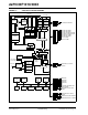
FIGURE 1-2: dsPIC30F2020 BLOCK DIAGRAM
Power-up
Timer
Oscillator
Start-up Timer
POR
Reset
Watchdog
Timer
Instruction
Decode &
Control
OSC1/CLK1
MCLR
AN4/CMP2C/CMP3A/CN6/RB4
UART1SPI1
SMPS
PWM
Timing
Generation
AN5/CMP2D/CMP3B/CN7/RB5
16
PCH PCL
Program Counter
ALU<16>
16
Address Latch
Program Memory
(12 Kbytes)
Data Latch
24
24
24
24
X Data Bus
IR
I
2
C™
Comparator
PCU
PWM1L/RE0
PWM1H/RE1
PWM2L/RE2
PWM2H/RE3
PWM3L/RE4
10-bit ADC
Timers
PWM3H/RE5
PGC1/EMUC1/EXTREF/PWM4L/
Input
Capture
Module
Output
Compare
Module
SFLT2/INT0/OCFLTA/RA9
PORTB
PGC/EMUC/SDI1/SDA/U1RX/RF7
PGD/EMUD/SD01/SCL/U1TX/RF8
PORTF
PORTD
16
16
16
16 x 16
W Reg Array
Divide
Unit
Engine
DSP
Decode
ROM Latch
16
Y Data Bus
Effective Address
X RAGU
X WAGU
Y AGU
AN0/CMP1A/CN2/RB0
AN1/CMP1B/CN3/RB1
AN2/CMP1C/CMP2A/CN4/RB2
AN3/CMP1D/CMP2B/CN5/RB3
16
16
16
16
16
PORTA
PORTE
16
16
16
16
8
Interrupt
Controller
PSV & Table
Data Access
Control Block
Stack
Control
Logic
Loop
Control
Logic
Data LatchData Latch
Y Data
(256 bytes)
RAM
X Data
(256 bytes)
RAM
Address
Latch
Address
Latch
Control Signals
to Various Blocks
PGC2/EMUC2/OC1/SFLT1/IC1/
16
16
AN6/CMP3C/CMP4A/
AN7/CMP3D/CMP4B/
OSC1/CLKI/RB6
OSC2/CLKO/RB7
INT1/RD0
PGD2/EMUD2/SCK1/SFLT3/OC2
/
INT2/RF6
PGD1/EMUD1/PWM4H/T2CK/
Module
Input
Change
Notification
U1ARX/CN0/RE6
U1ATX/CN1/RE7
T1CK/