
Datasheet


dsPIC30F1010/202X
DS70178C-page 128 Preliminary © 2006 Microchip Technology Inc.
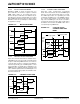
FIGURE 12-17: DUAL DEAD-TIME
WAVEFORMS
12.14.3 DEAD-TIME RANGES
The amount of dead time provided by each dead-time
unit is selected by specifying a 12-bit unsigned value in
the DTRx registers. The 12-bit dead-time counters
clock at four times the instruction execution rate. The
Least Significant one bit of the dead-time value are
processed by the Fine Adjust PWM module.
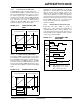
Table 12-3 shows example dead-time ranges as a
function of the device operating frequency.
TABLE 12-3: EXAMPLE DEAD-TIME
RANGES
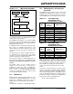
12.14.4 DEAD-TIME INSERTION TIMING
Figure 12-18 shows how the dead-time insertion for
complementary signals is accomplished.
12.14.5 DEAD-TIME DISTORTION
For small PWM duty cycles, the ratio of dead time to the
active PWM time may become large. In this case, the
inserted dead time introduces distortion into wave-
forms produced by the PWM module. The user can
ensure that dead-time distortion is minimized by keep-
ing the PWM duty cycle at least three times larger than
the dead time.
A similar effect occurs for duty cycles at or near 100%.
The maximum duty cycle used in the application should
be chosen such that the minimum inactive time of the
signal is at least three times larger than the dead time.
FIGURE 12-18: DEAD-TIME INSERTION (PWM OUTPUT SIGNAL TIMING MAY BE DELAYED)
PWMH
PWML
PWML
PWML
PWMH
PWMH
No dead time
Positive dead time
Negative dead time
DTRx
ALTDTRx
MIPS Resolution Dead-Time Range
30 4.16 ns 0-17.03 µsec
20 6.25 ns 0-25.59 µsec
90
123
4
5
6
78
CLOCK
PTMR
DUTY CYCLE REG
4
RAW PWMH
RAW PWML
PWMH OUTPUT
PWML OUTPUT
DEAD-TIME VALUE
1
<10:4>
<15:4>