
Datasheet


© 2006 Microchip Technology Inc. Preliminary DS70178C-page 119
dsPIC30F1010/202X
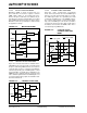
REGISTER 12-13: TRIGx: PWM TRIGGER COMPARE VALUE REGISTER
R/W-0 R/W-0 R/W-0 R/W-0 R/W-0 R/W-0 R/W-0 R/W-0
TRGCMP<15:8>
bit 15 bit 8
R/W-0 R/W-0 R/W-0 R/W-0 R/W-0 U-0 U-0 U-0
TRGCMP<7:3>
— — —
bit 7 bit 0
Legend:
R = Readable bit W = Writable bit U = Unimplemented bit, read as ‘0’
-n = Value at POR ‘1’ = Bit is set ‘0’ = Bit is cleared x = Bit is unknown
bit 15-3 TRGCMP<15:3>: Trigger Control Value bits
(1)
Register contains the compare value for PWMx time base for generating a trigger to the ADC module
for initiating a sample and conversion process, or generating a trigger interrupt.
bit 2-0 Unimplemented: Read as ‘0’
Note 1: The minimum usable value for this register is 0x0008
A value of 0x0000 does not produce a trigger.
If the TRIGx value is being calculated based on duty cycle value, you must ensure that a minimum TRIGx
value is written into the register at all times.