
Datasheet


© 2010 Microchip Technology Inc. DS70139G-page 63
dsPIC30F2011/2012/3012/3013
7.3 Input Change Notification Module
The input change notification module provides the
dsPIC30F devices the ability to generate interrupt
requests to the processor, in response to a change of
state on selected input pins. This module is capable of
detecting input change of states even in Sleep mode,
when the clocks are disabled. There are up to 10
external signals (CN0 through CN7, CN17 and CN18)
that may be selected (enabled) for generating an
interrupt request on a change of state.
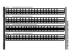
TABLE 7-7: INPUT CHANGE NOTIFICATION REGISTER MAP FOR dsPIC30F2011/3012 (BITS 7-0)
TABLE 7-8: INPUT CHANGE NOTIFICATION REGISTER MAP FOR dsPIC30F2012/3013 (BITS 7-0)
SFR
Name
Address Bit 7 Bit 6 Bit 5 Bit 4 Bit 3 Bit 2 Bit 1 Bit 0 Reset State
CNEN1 00C0 CN7IE CN6IE CN5IE CN4IE CN3IE CN2IE CN1IE CN0IE 0000 0000 0000 0000
CNEN2 00C2
— — — — — — — — 0000 0000 0000 0000
CNPU1 00C4 CN7PUE CN6PUE CN5PUE CN4PUE CN3PUE CN2PUE CN1PUE CN0PUE 0000 0000 0000 0000
CNPU2 00C6
— — — — — — — — 0000 0000 0000 0000
Legend: — = unimplemented bit, read as ‘0’
SFR
Name
Address Bit 7 Bit 6 Bit 5 Bit 4 Bit 3 Bit 2 Bit 1 Bit 0 Reset State
CNEN1 00C0 CN7IE CN6IE CN5IE CN4IE CN3IE CN2IE CN1IE CN0IE 0000 0000 0000 0000
CNEN2 00C2
— — — — — CN18IE CN17IE — 0000 0000 0000 0000
CNPU1 00C4 CN7PUE CN6PUE CN5PUE CN4PUE CN3PUE CN2PUE CN1PUE CN0PUE 0000 0000 0000 0000
CNPU2 00C6
— — — — — CN18PUE CN17PUE — 0000 0000 0000 0000
Legend: — = unimplemented bit, read as ‘0’
Note: Refer to the “dsPIC30F Family Reference Manual” (DS70046) for descriptions of register bit fields.