
Datasheet


dsPIC30F2011/2012/3012/3013
DS70139G-page 60 © 2010 Microchip Technology Inc.
7.2 Configuring Analog Port Pins
The use of the ADPCFG and TRIS registers control the
operation of the A/D port pins. The port pins that are
desired as analog inputs must have their
corresponding TRIS bit set (input). If the TRIS bit is
cleared (output), the digital output level (V
OH or VOL) is
converted.
When the PORT register is read, all pins configured as
analog input channels are read as cleared (a low level).
Pins configured as digital inputs will not convert an
analog input. Analog levels on any pin that is defined as
a digital input (including the ANx pins) may cause the
input buffer to consume the current that exceeds
device specifications.
7.2.1 I/O PORT WRITE/READ TIMING
One instruction cycle is required between a port
direction change or port write operation and a read
operation of the same port. Typically this instruction
would be a NOP.
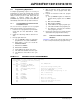
EXAMPLE 7-1: PORT WRITE/READ
EXAMPLE
MOV #0xF0, W0 ; Configure PORTB<7:4>
; as inputs
MOV W0, TRISB ; and PORTB<3:0> as outputs
NOP ; additional instruction
cycle
btss PORTB, #7 ; bit test RB7 and skip if
set