
Datasheet


dsPIC30F2011/2012/3012/3013
DS70139G-page 6 © 2010 Microchip Technology Inc.
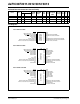
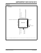
Pin Diagrams
10
11
2
3
6
1
18
19
20
21
22
12
13
14
15
8
7
16
17
23
24
25
26
27
28
9
dsPIC30F2012
EMUD1/SOSCI/T2CK/U1ATX/CN1/RC13
5
4
AVDD
AVSS
AN6/OCFA/RB6
EMUD2/AN7/RB7
AN8/OC1/RB8
AN9/OC2/RB9
CN17/RF4
CN18/RF5
V
DD
VSS
PGC/EMUC/U1RX/SDI1/SDA/RF2
PGD/EMUD/U1TX/SDO1/SCL/RF3
SCK1/INT0/RF6
EMUC2/IC1/INT1/RD8
MCLR
EMUD3/AN0/VREF+/CN2/RB0
EMUC3/AN1/V
REF-/CN3/RB1
AN2/SS1/LVDIN/CN4/RB2
AN3/CN5/RB3
AN4/CN6/RB4
AN5/CN7/RB5
V
SS
OSC1/CLKI
OSC2/CLKO/RC15
EMUC1/SOSCO/T1CK/U1ARX/CN0/RC14
V
DD
IC2/INT2/RD9
28-Pin QFN-S
(1)
Note 1: The metal plane at the bottom of the device is not connected to any pins and is recommended to be connected to VSS externally.