
Datasheet


© 2010 Microchip Technology Inc. DS70139G-page 59
dsPIC30F2011/2012/3012/3013
7.0 I/O PORTS
All of the device pins (except VDD, VSS, MCLR and
OSC1/CLKI) are shared between the peripherals and
the parallel I/O ports.
All I/O input ports feature Schmitt Trigger inputs for
improved noise immunity.
7.1 Parallel I/O (PIO) Ports
When a peripheral is enabled and the peripheral is
actively driving an associated pin, the use of the pin as
a general purpose output pin is disabled. The I/O pin
can be read, but the output driver for the parallel port bit
is disabled. If a peripheral is enabled, but the peripheral
is not actively driving a pin, that pin can be driven by a
port.
All port pins have three registers directly associated
with the operation of the port pin. The Data Direction
register (TRISx) determines whether the pin is an input
or an output. If the data direction bit is a ‘1’, then the pin
is an input. All port pins are defined as inputs after a
Reset. Reads from the latch (LATx), read the latch.
Writes to the latch, write the latch (LATx). Reads from
the port (PORTx), read the port pins and writes to the
port pins, write the latch (LATx).
Any bit and its associated data and Control registers
that are not valid for a particular device are disabled.
That means the corresponding LATx and TRISx
registers and the port pin read as zeros.
When a pin is shared with another peripheral or
function that is defined as an input only, it is
nevertheless regarded as a dedicated port because
there is no other competing source of outputs.
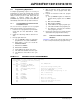
A parallel I/O (PIO) port that shares a pin with a
peripheral is, in general, subservient to the peripheral.
The peripheral’s output buffer data and control signals
are provided to a pair of multiplexers. The multiplexers
select whether the peripheral or the associated port
has ownership of the output data and control signals of
the I/O pad cell. Figure 7-1 illustrates how ports are
shared with other peripherals and the associated I/O
cell (pad) to which they are connected.
The format of the registers for the shared ports,
(PORTB, PORTC, PORTD and PORTF) are shown in
Table 7-1 through Table 7-6.
FIGURE 7-1: BLOCK DIAGRAM OF A SHARED PORT STRUCTURE
Note: This data sheet summarizes features of
this group of dsPIC30F devices and is not
intended to be a complete reference
source. For more information on the CPU,
peripherals, register descriptions and
general device functionality, refer to the
“dsPIC30F Family Reference Manual”
(DS70046).
Note: The actual bits in use vary between
devices.
QD
CK
WR LAT +
TRIS Latch
I/O Pad
WR Port
Data Bus
QD
CK
Data Latch
Read LAT
Read Port
Read TRIS
1
0
1
0
WR TRIS
Peripheral Output Data
Output Enable
Peripheral Input Data
I/O Cell
Peripheral Module
Peripheral Output Enable
PIO Module
Output Multiplexers
Output Data
Input Data
Peripheral Module Enable