
Datasheet


© 2010 Microchip Technology Inc. DS70139G-page 19
dsPIC30F2011/2012/3012/3013
2.0 CPU ARCHITECTURE
OVERVIEW
This section is an overview of the CPU architecture of
the dsPIC30F. The core has a 24-bit instruction word.
The Program Counter (PC) is 23 bits wide with the
Least Significant bit (LSb) always clear (see
Section 3.1 “Program Address Space”). The Most
Significant bit (MSb) is ignored during normal program
execution, except for certain specialized instructions.
Thus, the PC can address up to 4M instruction words
of user program space. An instruction prefetch
mechanism helps maintain throughput. Program loop
constructs, free from loop count management
overhead, are supported using the DO and REPEAT
instructions, both of which are interruptible at any point.
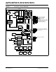
2.1 Core Overview
The working register array consists of 16 x 16-bit
registers, each of which can act as data, address or
offset registers. One working register (W15) operates
as a Software Stack Pointer for interrupts and calls.
The data space is 64 Kbytes (32K words) and is split
into two blocks, referred to as X and Y data memory.
Each block has its own independent Address Genera-
tion Unit (AGU). Most instructions operate solely
through the X memory, AGU, which provides the
appearance of a single unified data space. The
Multiply-Accumulate (MAC) class of dual source DSP
instructions operate through both the X and Y AGUs,
splitting the data address space into two parts (see
Section 3.2 “Data Address Space”). The X and Y
data space boundary is device specific and cannot be
altered by the user. Each data word consists of 2 bytes
and most instructions can address data either as words
or bytes.
Two ways to access data in program memory are:
• The upper 32 Kbytes of data space memory can
be mapped into the lower half (user space) of
program space at any 16K program word
boundary, defined by the 8-bit Program Space
Visibility Page register (PSVPAG). Thus any
instruction can access program space as if it were
data space, with a limitation that the access
requires an additional cycle. Only the lower 16
bits of each instruction word can be accessed
using this method.
• Linear indirect access of 32K word pages within
program space is also possible using any working
register, via table read and write instructions.
Table read and write instructions can be used to
access all 24 bits of an instruction word.
Overhead-free circular buffers (Modulo Addressing)
are supported in both X and Y address spaces. This is
primarily intended to remove the loop overhead for
DSP algorithms.
The X AGU also supports Bit-Reversed Addressing on
destination effective addresses to greatly simplify input
or output data reordering for radix-2 FFT algorithms.
Refer to Section 4.0 “Address Generator Units” for
details on Modulo and Bit-Reversed Addressing.
The core supports Inherent (no operand), Relative,
Literal, Memory Direct, Register Direct, Register
Indirect, Register Offset and Literal Offset Addressing
modes. Instructions are associated with pre-defined
addressing modes, depending upon their functional
requirements.
For most instructions, the core is capable of executing
a data (or program data) memory read, a working
register (data) read, a data memory write and a
program (instruction) memory read per instruction
cycle. As a result, 3 operand instructions are
supported, allowing C = A+B operations to be exe-
cuted in a single cycle.
A DSP engine has been included to significantly
enhance the core arithmetic capability and throughput.
It features a high-speed 17-bit by 17-bit multiplier, a
40-bit ALU, two 40-bit saturating accumulators and a
40-bit bidirectional barrel shifter. Data in the
accumulator or any working register can be shifted up
to 15 bits right, or 16 bits left in a single cycle. The DSP
instructions operate seamlessly with all other
instructions and have been designed for optimal
real-time performance. The MAC class of instructions
can concurrently fetch two data operands from memory
while multiplying two W registers. To enable this
concurrent fetching of data operands, the data space
has been split for these instructions and linear is for all
others. This has been achieved in a transparent and
flexible manner, by dedicating certain working registers
to each address space for the MAC class of
instructions.
Note: This data sheet summarizes features of
this group of dsPIC30F devices and is not
intended to be a complete reference
source. For more information on the CPU,
peripherals, register descriptions and
general device functionality, refer to the
“dsPIC30F Family Reference Manual”
(DS70046). For more information on the
device instruction set and programming,
refer to the “16-bit MCU and DSC
Programmer’s Reference Manual”
(DS70157).