
Datasheet


dsPIC30F2011/2012/3012/3013
DS70139G-page 164 © 2010 Microchip Technology Inc.
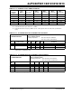
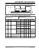
FIGURE 20-5: CLKO AND I/O TIMING CHARACTERISTICS
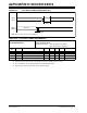
TABLE 20-20: CLKO AND I/O TIMING REQUIREMENTS
AC CHARACTERISTICS
Standard Operating Conditions: 2.5V to 5.5V
(unless otherwise stated)
Operating temperature -40°C ≤ TA ≤ +85°C for Industrial
-40°C ≤ T
A ≤ +125°C for Extended
Param
No.
Symbol Characteristic
(1)(2)(3)
Min Typ
(4)
Max Units Conditions
DO31 TIOR Port output rise time — 7 20 ns
DO32 T
IOF Port output fall time — 7 20 ns
DI35 TINP INTx pin high or low time (output) 20 — — ns
DI40 T
RBP CNx high or low time (input) 2 TCY ——ns
Note 1: These parameters are asynchronous events not related to any internal clock edges
2: Measurements are taken in RC mode and EC mode where CLKO output is 4 x TOSC.
3: These parameters are characterized but not tested in manufacturing.
4: Data in “Typ” column is at 5V, 25°C unless otherwise stated.
Note: Refer to Figure 20-3 for load conditions.
I/O Pin
(Input)
I/O Pin
(Output)
DI35
Old Value
New Value
DI40
DO31
DO32