
Datasheet


dsPIC30F2011/2012/3012/3013
DS70139G-page 14 © 2010 Microchip Technology Inc.
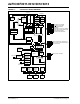
FIGURE 1-3: dsPIC30F3012 BLOCK DIAGRAM
Power-up
Timer
Oscillator
Start-up Timer
POR/BOR
Reset
Watchdog
Timer
Instruction
Decode &
Control
OSC1/CLKI
MCLR
V
DD
, V
SS
PGD/EMUD/AN4/U1TX/SDO1/SCL/CN6/RB4
Low-Voltage
Detect
UART1
Timing
Generation
PGC/EMUC/AN5/U1RX/SDI1/SDA/CN7/R
B5
16
PCH PCL
Program Counter
ALU<16>
16
24
24
24
24
X Data Bus
IR
I
2
C™
AN6/SCK1/INT0/OCFA/RB6
EMUD2/AN7/OC2/IC2/INT2/RB7
PCU
12-bit ADC
Timers
Input
Capture
Module
Output
Compare
Module
EMUC1/SOSCO/T1CK/U1ARX/CN0/RC14
EMUD1/SOSCI/T2CK/U1ATX/CN1/RC13
PORTB
PORTD
16
16
16
16 x 16
W Reg Array
Divide
Unit
Engine
DSP
Decode
ROM Latch
16
Y Data Bus
Effective Address
X RAGU
X WAGU
Y AGU
EMUD3/AN0/V
REF
+/CN2/RB0
EMUC3/AN1/V
REF
-/CN3/RB1
AN2/SS1/LVDIN/CN4/RB2
AN3/CN5/RB3
OSC2/CLKO/RC15
AV
DD
, AV
SS
16
16
16
16
16
PORTC
16
16
16
16
8
Interrupt
Controller
PSV & Table
Data Access
Control Block
Stack
Control
Logic
Loop
Control
Logic
Data LatchData Latch
Y Data
(1 Kbytes)
RAM
X Data
(1 Kbytes)
RAM
Address
Latch
Address
Latch
EMUC2/OC1/IC1/INT1/RD0
16
SPI1
Address Latch
Program Memory
(24 Kbytes)
Data Latch
16
Data EEPROM
(1 Kbytes)