
Datasheet


dsPIC30F2011/2012/3012/3013
DS70139G-page 136 © 2010 Microchip Technology Inc.
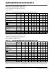
TABLE 17-7: SYSTEM INTEGRATION REGISTER MAP
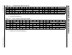
TABLE 17-8: DEVICE CONFIGURATION REGISTER MAP
SFR
Name
Address Bit 15 Bit 14 Bit 13 Bit 12 Bit 11 Bit 10 Bit 9 Bit 8 Bit 7 Bit 6 Bit 5 Bit 4 Bit 3 Bit 2 Bit 1 Bit 0 Reset State
RCON 0740 TRAPR IOPUWR BGST LVDEN LVDL<3:0> EXTR SWR SWDTEN WDTO SLEEP IDLE BOR POR (Note 1)
OSCCON 0742
—COSC<2:0>— NOSC<2:0> POST<1:0> LOCK —CF— LPOSCEN OSWEN (Note 2)
OSCTUN 0744
— — — — — — — — — — — — TUN3 TUN2 TUN1 TUN0 (Note 2)
PMD1 0770
— — T3MD T2MD T1MD — — — I2CMD U2MD
(3)
U1MD — SPI1MD — — ADCMD 0000 0000 0000 0000
PMD2 0772
— — — — — —IC2MDIC1MD— — — — — —OC2MDOC1MD0000 0000 0000 0000
Legend: — = unimplemented bit, read as ‘0’
Note 1: Reset state depends on type of reset.
2: Reset state depends on Configuration bits.
3: Only available on dsPIC30F3013 devices.
Name Address Bit 15 Bit 14 Bit 13 Bit 12 Bit 11 Bit 10 Bit 9 Bit 8 Bit 7 Bit 6 Bit 5 Bit 4 Bit 3 Bit 2 Bit 1 Bit 0
FOSC F80000 FCKSM<1:0>
— — — FOS<2:0> — — — FPR<4:0>
FWDT F80002 FWDTEN
— — — — — — — — — FWPSA<1:0> FWPSB<3:0>
FBORPOR F80004 MCLREN
— — — —
PWMPIN
(1)
HPOL
(1)
LPOL
(1)
BOREN —BORV<1:0>— —FPWRT<1:0>
FBS F80006
— — Reserved
(2)
— — — Reserved
(2)
— — — — Reserved
(2)
FSS F80008 — — Reserved
(2)
— — Reserved
(2)
— — — — Reserved
(2)
FGS F8000A — — — — — — — — — — — — — Reserved
(3)
GCP GWRP
FICD F8000C BKBUG COE
— — — — — — — — — — — —ICS<1:0>
Legend: — = unimplemented bit, read as ‘0’
Note 1: These bits are reserved (read as ‘1’ and must be programmed as ‘1’).
2: Reserved bits read as ‘1’ and must be programmed as ‘1’.
3: The FGS<2> bit is a read-only copy of the GCP bit (FGS<1>).