
Datasheet


dsPIC30F2011/2012/3012/3013
DS70139G-page 134 © 2010 Microchip Technology Inc.
Any interrupt that is individually enabled (using the
corresponding IE bit) and meets the prevailing priority
level will be able to wake-up the processor. The
processor will process the interrupt and branch to the
ISR. The Sleep Status bit in the RCON register is set
upon wake-up.
All Resets will wake-up the processor from Sleep
mode. Any Reset, other than POR, will set the Sleep
Status bit. In a POR, the Sleep bit is cleared.
If the Watchdog Timer is enabled, then the processor
will wake-up from Sleep mode upon WDT time-out. The
Sleep and WDTO Status bits are both set.
17.6.2 IDLE MODE
In Idle mode, the clock to the CPU is shut down while
peripherals keep running. Unlike Sleep mode, the clock
source remains active.
Several peripherals have a control bit in each module
that allows them to operate during Idle.
LPRC Fail-Safe Clock remains active if clock failure
detect is enabled.
The processor wakes up from Idle if at least one of the
following conditions has occurred:
• any interrupt that is individually enabled (IE bit is
‘1’) and meets the required priority level
• any Reset (POR, BOR, MCLR
)
• WDT time-out
Upon wake-up from Idle mode, the clock is re-applied
to the CPU and instruction execution begins
immediately, starting with the instruction following the
PWRSAV instruction.
Any interrupt that is individually enabled (using IE bit)
and meets the prevailing priority level will be able to
wake-up the processor. The processor will process the
interrupt and branch to the ISR. The Idle Status bit in
the RCON register is set upon wake-up.
Any Reset other than POR will set the Idle Status bit.
On a POR, the Idle bit is cleared.
If Watchdog Timer is enabled, then the processor will
wake-up from Idle mode upon WDT time-out. The Idle
and WDTO Status bits are both set.
Unlike wake-up from Sleep, there are no time delays
involved in wake-up from Idle.
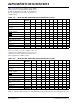
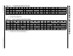
17.7 Device Configuration Registers
The Configuration bits in each device Configuration
register specify some of the device modes and are
programmed by a device programmer, or by using the
In-Circuit Serial Programming™ (ICSP™) feature of
the device. Each device Configuration register is a
24-bit register, but only the lower 16 bits of each
register are used to hold configuration data. There are
five device Configuration registers available to the
user:
1. FOSC (0xF80000): Oscillator Configuration
Register
2. FWDT (0xF80002): Watchdog Timer
Configuration Register
3. FBORPOR (0xF80004): BOR and POR
Configuration Register
4. FGS (0xF8000A): General Code Segment
Configuration Register
5. FICD (0xF8000C): Debug Configuration
Register
The placement of the Configuration bits is
automatically handled when you select the device in
your device programmer. The desired state of the
Configuration bits may be specified in the source code
(dependent on the language tool used), or through the
programming interface. After the device has been
programmed, the application software may read the
Configuration bit values through the table read
instructions. For additional information, please refer to
the Programming Specifications of the device.
Note: In spite of various delays applied (T
POR,
T
LOCK and TPWRT), the crystal oscillator
(and PLL) may not be active at the end of
the time-out (e.g., for low-frequency
crystals). In such cases, if FSCM is
enabled, then the device will detect this as
a clock failure and process the clock failure
trap, the FRC oscillator will be enabled and
the user will have to re-enable the crystal
oscillator. If FSCM is not enabled, then the
device will simply suspend execution of
code until the clock is stable and will remain
in Sleep until the oscillator clock has
started.
Note: If the code protection Configuration fuse
bits (FGS<GCP> and FGS<GWRP>)
have been programmed, an erase of the
entire code-protected device is only
possible at voltages V
DD ≥ 4.5V.