
Datasheet


© 2010 Microchip Technology Inc. DS70139G-page 129
dsPIC30F2011/2012/3012/3013
17.3 Reset
The dsPIC30F2011/2012/3012/3013 devices
differentiate between various kinds of Reset:
a) Power-on Reset (POR)
b) MCLR
Reset during normal operation
c) MCLR
Reset during Sleep
d) Watchdog Timer (WDT) Reset (during normal
operation)
e) Programmable Brown-out Reset (BOR)
f) RESET Instruction
g) Reset caused by trap lockup (TRAPR)
h) Reset caused by illegal opcode or by using an
uninitialized W register as an address pointer
(IOPUWR)
Different registers are affected in different ways by
various Reset conditions. Most registers are not
affected by a WDT wake-up since this is viewed as the
resumption of normal operation. Status bits from the
RCON register are set or cleared differently in different
Reset situations, as indicated in Table 17-5. These bits
are used in software to determine the nature of the
Reset.
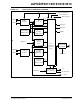
A block diagram of the On-Chip Reset Circuit is shown
in Figure 17-2.
A MCLR
noise filter is provided in the MCLR Reset
path. The filter detects and ignores small pulses.
Internally generated Resets do not drive MCLR
pin low.
17.3.1 POR: POWER-ON RESET
A power-on event will generate an internal POR pulse
when a V
DD rise is detected. The Reset pulse will occur
at the POR circuit threshold voltage (VPOR) which is
nominally 1.85V. The device supply voltage
characteristics must meet specified starting voltage
and rise rate requirements. The POR pulse will reset a
POR timer and place the device in the Reset state. The
POR also selects the device clock source identified by
the oscillator configuration fuses.
The POR circuit inserts a small delay, T
POR, which is
nominally 10 μs and ensures that the device bias
circuits are stable. Furthermore, a user selected
power-up time-out (T
PWRT) is applied. The TPWRT
parameter is based on device Configuration bits and
can be 0 ms (no delay), 4 ms, 16 ms or 64 ms. The total
delay is at device power-up, TPOR + TPWRT. When
these delays have expired, SYSRST
will be negated on
the next leading edge of the Q1 clock and the PC will
jump to the Reset vector.
The timing for the SYSRST
signal is shown in
Figure 17-3 through Figure 17-5.
FIGURE 17-2: RESET SYSTEM BLOCK DIAGRAM
S
R
Q
MCLR
VDD
VDD Rise
Detect
POR
SYSRST
Sleep or Idle
Brown-out
Reset
BOREN
RESET
Instruction
WDT
Module
Digital
Glitch Filter
BOR
Trap Conflict
Illegal Opcode/
Uninitialized W Register