
Datasheet


dsPIC30F2011/2012/3012/3013
DS70139G-page 126 © 2010 Microchip Technology Inc.
17.2 Oscillator Configurations
17.2.1 INITIAL CLOCK SOURCE
SELECTION
While coming out of Power-on Reset or Brown-out
Reset, the device selects its clock source based on:
a) FOS<2:0> Configuration bits that select one of
four oscillator groups,
b) and FPR<4:0> Configuration bits that select one
of 15 oscillator choices within the primary group.
The selection is as shown in Table 17-2.
17.2.2 OSCILLATOR START-UP TIMER
(OST)
In order to ensure that a crystal oscillator (or ceramic
resonator) has started and stabilized, an Oscillator
Start-up Timer is included. It is a simple 10-bit counter
that counts 1024 T
OSC cycles before releasing the
oscillator clock to the rest of the system. The time-out
period is designated as T
OST.
The T
OST time is involved every time the oscillator has
to restart (i.e., on POR, BOR and wake-up from Sleep).
The Oscillator Start-up Timer is applied to the LP
oscillator, XT, XTL and HS modes (upon wake-up from
Sleep, POR and BOR) for the primary oscillator.
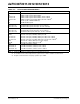
TABLE 17-2: CONFIGURATION BIT VALUES FOR CLOCK SELECTION
Oscillator Mode
Oscillator
Source
FOS<2:0> FPR<4:0>
OSC2
Function
ECIO w/PLL 4x PLL
1 1 101101 I/O
ECIO w/PLL 8x PLL
1 1 101110 I/O
ECIO w/PLL 16x PLL
1 1 101111 I/O
FRC w/PLL 4X PLL 1 1 100001 I/O
FRC w/PLL 8x PLL
1 1 101010 I/O
FRC w/PLL 16x PLL
1 1 100011 I/O
XT w/PLL 4x PLL 1 1 100101 OSC2
XT w/PLL 8x PLL
1 1 100110 OSC2
XT w/PLL 16x PLL
1 1 100111 OSC2
HS2 w/PLL 4x PLL 1 1 110001 OSC2
HS2 w/PLL 8x PLL
1 1 110010 OSC2
HS2 w/ PLL 16x PLL
1 1 110011 OSC2
HS3 w/PLL 4x PLL 1 1 110101 OSC2
HS3 w/PLL 8x PLL
1 1 110110 OSC2
HS3 w/PLL 16x PLL
1 1 110111 OSC2
ECIO External 0 1 101100 I/O
XT External
0 1 100100 OSC2
HS External
0 1 100010 OSC2
EC External
0 1 101011 CLKO
ERC External
0 1 101001 CLKO
ERCIO External
0 1 101000 I/O
XTL External 0 1 100000 OSC2
LP Secondary
0 0 0XXXXX(Note 1, 2)
FRC Internal FRC
0 0 1XXXXX(Note 1, 2)
LPRC Internal LPRC 0 1 0XXXXX(Note 1, 2)
Note 1: The OSC2 pin is either usable as a general purpose I/O pin or is completely unusable, depending on the
Primary Oscillator mode selection (FPR<4:0>).
2: OSC1 pin cannot be used as an I/O pin even if the secondary oscillator or an internal clock source is
selected at all times.