
Datasheet


© 2010 Microchip Technology Inc. DS70139G-page 113
dsPIC30F2011/2012/3012/3013
16.0 12-BIT ANALOG-TO-DIGITAL
CONVERTER (ADC) MODULE
The 12-bit Analog-to-Digital Converter allows
conversion of an analog input signal to a 12-bit digital
number. This module is based on a Successive
Approximation Register (SAR) architecture and
provides a maximum sampling rate of 200 ksps. The
ADC module has up to 10 analog inputs which are
multiplexed into a sample and hold amplifier. The
output of the sample and hold is the input into the
converter which generates the result. The analog
reference voltage is software selectable to either the
device supply voltage (AV
DD/AVSS) or the voltage level
on the (V
REF+/VREF-) pin. The ADC has a unique
feature of being able to operate while the device is in
Sleep mode with RC oscillator selection.
The ADC module has six 16-bit registers:
• A/D Control Register 1 (ADCON1)
• A/D Control Register 2 (ADCON2)
• A/D Control Register 3 (ADCON3)
• A/D Input Select Register (ADCHS)
• A/D Port Configuration Register (ADPCFG)
• A/D Input Scan Selection Register (ADCSSL)
The ADCON1, ADCON2 and ADCON3 registers
control the operation of the ADC module. The ADCHS
register selects the input channels to be converted. The
ADPCFG register configures the port pins as analog
inputs or as digital I/O. The ADCSSL register selects
inputs for scanning.
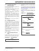
The block diagram of the 12-bit ADC module is shown
in Figure 16-1.
FIGURE 16-1: 12-BIT ADC FUNCTIONAL BLOCK DIAGRAM
Note: This data sheet summarizes features of
this group of dsPIC30F devices and is not
intended to be a complete reference
source. For more information on the CPU,
peripherals, register descriptions and
general device functionality, refer to the
“dsPIC30F Family Reference Manual”
(DS70046).
Note: The SSRC<2:0>, ASAM, SMPI<3:0>,
BUFM and ALTS bits, as well as the
ADCON3 and ADCSSL registers, must
not be written to while ADON = 1. This
would lead to indeterminate results.
Comparator
12-bit SAR Conversion Logic
AVDD/VREF+
DAC
Data Format
16-word, 12-bit
Dual Port
Buffer
Bus Interface
0000
0101
0111
1001
0001
0010
0011
0100
0110
1000
AN8
AN9
AN4
AN5
AN6
AN7
AN0
AN1
AN2
AN3
CH0
AVSS/VREF-
Sample/Sequence
Control
Sample
Input MUX
Control
Input
Switches
S/H