
Datasheet


© 2011 Microchip Technology Inc. DS70118J-page 133
dsPIC30F2010
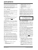
TABLE 19-7: SYSTEM INTEGRATION REGISTER MAP
(1)
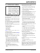
TABLE 19-8: DEVICE CONFIGURATION REGISTER MAP
(1)
SFR Name Addr. Bit 15 Bit 14 Bit 13 Bit 12 Bit 11 Bit 10 Bit 9 Bit 8 Bit 7 Bit 6 Bit 5 Bit 4 Bit 3 Bit 2 Bit 1 Bit 0 Reset State
RCON 0740 TRAPR IOPUWR BGST
— — — — — EXTR SWR SWDTEN WDTO SLEEP IDLE BOR POR Depends on type of Reset
OSCCON 0742 TUN3 TUN2 COSC<1:0> TUN1 TUN0 NOSC<1:0> POST<1:0> LOCK
—CF— LPOSCEN OSWEN Depends on Configuration bits
Legend: — = unimplemented bit
Note 1: Refer to the “dsPIC30F Family Reference Manual” (DS70046) for descriptions of register bit fields.
Name Address Bit 15 Bit 14 Bit 13 Bit 12 Bit 11 Bit 10 Bit 9 Bit 8 Bit 7 Bit 6 Bit 5 Bit 4 Bit 3 Bit 2 Bit 1 Bit 0
FOSC F80000 FCKSM<1:0>
— — — — FOS<1:0> — — — —FPR<3:0>
FWDT F80002 FWDTEN
— — — — — — — — — FWPSA<1:0> FWPSB<3:0>
FBORPOR F80004 MCLREN
— — — —
PWMPIN
HPOL LPOL BOREN — BORV<1:0> — —FPWRT<1:0>
FBS F80006
— — Reserved
(2)
— — — Reserved
(2)
— — — —Reserved
(2)
FSS F80008 — — Reserved
(2)
— — Reserved
(2)
— — — —Reserved
(2)
FGS F8000A — — — — — — — — — — — — —
Reserved
(2)
GCP GWRP
FICD F8000C BKBUG COE
— — — — — — — — — — — —ICS<1:0>
Legend: — = unimplemented bit
Note 1: Refer to the “dsPIC30F Family Reference Manual” (DS70046) for descriptions of register bit fields.
2: Reserved bits read as ‘1’ and must be programmed as ‘1’.