
User`s guide
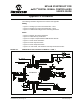


MPLAB STARTER KIT FOR
dsPIC
®
DIGITAL SIGNAL CONTROLLERS
USER’S GUIDE
© 2008 Microchip Technology Inc. DS51700A-page 31
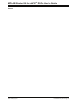
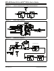
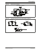
Appendix A. Schematics
The following schematic diagrams are included in this appendix:
Debug
• Figure A-1: Debug Input and Control Schematic – Part 1
• Figure A-2: Debug Input and Control Schematic – Part 2
• Figure A-3: USB Interface/Target Power Switching Schematic
Audio
• Figure A-4: Speech Processing Schematic
• Figure A-5: Flash Memory Schematics
• Figure A-6: Output Compare Module PWM Filters Schematic
• Figure A-7: Audio Codec Schematic
• Figure A-8: Audio Input Schematic
• Figure A-9: Audio Output Schematic
• Figure A-10: User LEDs, User Switches and Temp Sensor Schematics
FIGURE A-1: DEBUG INPUT AND CONTROL SCHEMATIC – PART 1
PIC18F67J50