
User manual


MPLAB Starter Kit for PIC24F User’s Guide
DS51725A-page 30 © 2008 Microchip Technology Inc.
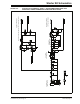
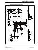
D5. Low VCE Saturation PNP Transistor Switch (Q1): Provides target power (via
high-side switching) to the application side components via control by the
PIC18F67J50.
D6. Debugger/Programmer Clock Crystal (Y1): Provides an accurate 12 MHz
frequency reference for the PIC18F67J50 microcontroller for stable USB
operations in Programming and Debugging modes. The PIC18F67J50 also uses
this to generate a second 12 MHz clock for use by the PIC24FJ256GB106
microcontroller.
D7. 25LC010A Serial EEPROM (U3): Provides nonvolatile parameter storage for
the PIC18F67J50.
D8. V
BUS and GND Test Points: These unpopulated pads may be equipped with
appropriate connectors and furnished with power to operate the board in
Stand-Alone mode.
D9. System Power LED (D2): When lit, indicates that the starter kit is powered via
the USB.
D10. Debug LED (D3): When lit, indicates that communication between the starter
kit and MPLAB IDE has been successfully established.
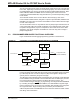
5.3.2 Application Components
The components listed here (in order of their reference tags in Figure 5-3) are the key
components of the application side of the starter kit:
A1. PIC24F256GB106 Microcontroller (U6): This provides the processing power
for the demo applications and application development on the starter kit.
The microcontroller features 256 Kbytes of Flash program memory and
16 Kbytes RAM.
The demo application uses an external 12 MHz signal from the programmer side
as clock source. Custom applications that do not use the USB module may also
use the microcontroller’s on-chip FRC oscillator as a clock source. (USB appli-
cations must use the 12 MHz programmer clock source, as the tolerance of the
FRC oscillator exceeds USB specifications.)
A2. Tri-Color LED Pads (D6, D10 or D11): One of these locations is populated with
a three-channel (RGB) LED; the choice of the populated site depends on the
availability of components at the time of the board’s assembly. Functionally, the
LEDs at any of these sites are interchangeable.
A3. OLED Display (LED1): A 128 x 64 pixel, monochrome organic LED array
provides a wide range of graphics and alphanumeric display options.
A4. Capacitive Touch Pad (S1): This 5-element keypad is an integral part of the
board’s top layer. The application responds to capacitive changes induced by
direct contact with the user by monitoring each of the touch pad’s elements with
the microcontroller’s integrated CTMU module.
A5. RTCC Crystal (Y2): Provides an accurate 32.768 kHz reference for the micro-
controller’s secondary oscillator. This is used in turn as the time base for the
on-chip Real-Time Clock (RTC).
A6. USB A Receptacle (J4): The application uses this receptacle to connect with
USB peripherals while operating as an embedded host.
A7. Mini-B USB Receptacle (J5): Physically identical to J1, this provides USB con-
nectivity for the application side when it is functioning as a peripheral device.
A8. Potentiometer (R44): Provides an analog input to the microcontroller for certain
demo applications.
A9. OLED Voltage Boost Circuitry: L3, D5 and Q4 (along with other passive
components) are connected in a voltage boost topology. This provides the OLED
display with its nominal operating voltage of 13 V
DC.