
User manual


Table Of Contents
- Chapter 1. Overview
- 1.1 Introduction
- 1.2 Highlights
- 1.3 PICDEM™ Lab Development Kit Contents
- 1.4 PICDEM™ Lab Development Board Construction and Layout
- 1.5 Target Power
- 1.6 Connecting the PICkit™ 2 Programmer/Debugger
- 1.7 Solderless Prototyping Area Strip Configuration
- Chapter 2. Getting Started
- 2.1 Introduction
- 2.2 Prerequisites
- 2.3 The Software Control Loop
- 2.4 MPLAB® IDE Download Instructions
- 2.5 Installing the Included Lab Files
- Chapter 3. General Purpose Input/Output Labs
- 3.1 Introduction
- 3.2 General Purpose Input/Output Labs
- 3.3 GPIO Output Labs
- 3.3.1 Reference Documentation
- 3.3.2 Equipment Required for GPIO Output Labs
- 3.3.3 PICDEM Lab Development Board Setup for GPIO Output Labs
- Figure 3-1: PICDEM Lab Schematic for GPIO Output Labs
- 3.3.4 Lab 1: Light LEDs
- Figure 3-2: MAIN() Software Control Loop Flowchart for Lab 1
- Figure 3-3: Step One
- Figure 3-4: Step Two
- Figure 3-5: Step Three
- Figure 3-6: Step Four
- Figure 3-7: Summary
- Figure 3-8: Project Window
- Figure 3-9: PICkit 2 PROGRAMMER/DEBUGGER TOOLBAR
- Figure 3-10: Lab 1 LED Output
- 3.3.5 Lab 2: Flash LEDs (Delay Loop)
- Figure 3-11: Main() Software Control Loop Flowchart for Lab 2
- Figure 3-12: Timing() Delay Routine Flowchart for Lab 2
- 3.3.6 Lab 3: Simple Delays Using Timer0
- Equation 3-1: TMR0 Overflow Period using FOSC/4
- Equation 3-2: TMR0 Overflow Period when including the Prescaler
- Equation 3-3: Calculating a TMR0 PreLoad Value to generate a 10mS Overflow Period
- Figure 3-13: Delay_10mS() using Timer0
- Equation 3-4: Maximum TMR0 Overflow Period
- Figure 3-14: Delay_1S() using Timer0
- 3.3.7 Lab 4: Rotate LEDs
- Figure 3-15: Main() Software Control Loop Flowchart for Lab 4
- Figure 3-16: Decide() Flowchart for Lab 4
- Figure 3-17: Results of Do_Output()
- 3.4 GPIO Input Labs
- 3.4.1 Reference Documentation
- 3.4.2 Equipment Required for GPIO Input Labs
- 3.4.3 PICDEM Lab Development Board Setup for GPIO Input Labs
- Figure 3-18: PICDEM Lab Schematic for GPIO Input Labs
- 3.4.4 Lab 5: Adding a Push Button
- Figure 3-19: Main() Software Control Loop Flowchart for Lab 5
- Figure 3-20: Get_Inputs() Software Flowchart for Lab 5
- Figure 3-21: Delay_5mS() Software Flowchart for Lab 5
- Figure 3-22: Decide() Software FlowChart for Lab 5
- 3.4.5 Lab 6: Push Button Interrupt
- Figure 3-23: Main() Software Control Loop Flowchart for GPIO Lab 6
- Figure 3-24: pb_pressISR() for Lab 6 Showing Switch Debounce
- 3.4.6 Lab 7: Push Button Interrupt-on-Change
- Figure 3-25: pb_pressisr Flowchart for Lab 7
- 3.4.7 Lab 8: Using Weak Pull-Ups
- Chapter 4. Comparator Peripheral Labs
- 4.1 Introduction
- 4.2 Comparator Labs
- 4.2.1 Reference Documentation
- 4.2.2 Comparator Labs
- 4.2.3 Equipment Required
- 4.2.4 Lab 1: Simple Compare
- Figure 4-1: Schematic for Comparator Lab 1
- Figure 4-2: Main() software Control Loop Flowchart for Comparator Lab 1
- 4.2.5 Lab 2: Using the Comparator Voltage Reference
- Equation 4-1: CVref Output Voltage
- Equation 4-2: Calculating a 2.5V Internal Reference (Low-Range Method)
- Figure 4-3: Schematic for Comparator Lab 2
- 4.2.6 Lab 3: Higher Resolution Sensor Readings Using a Single Comparator
- Figure 4-4: Basic Relaxation Oscillator Circuit
- Figure 4-5: Schematic for Comparator Lab 3
- Figure 4-6: Main() software Control Loop Flowchart for Comparator Lab 3
- Figure 4-7: TMR0_ISR Flowchart for Comparator Lab 3
- Chapter 5. Analog-to-Digital Converter Peripheral Labs
- 5.1 Introduction
- 5.2 ADC Labs
- Figure 5-1: Schematic for ADC Lab 1
- Figure 5-2: Main() software Control Loop Flowchart for Comparator Lab 1
- Figure 5-3: Main() software Control Loop Flowchart for Comparator Lab 1
- Figure 5-4: ADC Result Bit Significance
- Figure 5-5: Schematic for ADC Lab 2
- Figure 5-6: Main() software Control Loop Flowchart for ADC Lab 2
- Appendix A. Schematic
- Worldwide Sales
PICDEM
TM
Lab Development Board User’s Guide
DS41369A-page 86 © 2009 Microchip Technology Inc.
The audible frequency range is between 20-20000Hz. Therefore, the Timing()
delays from a maximum of 4.096 mS (244.1Hz) to a minimum of 1.536 mS (651Hz).
These values are determined using the internal instruction clock (F
OSC/4) as the TMR0
clock source with a prescaler of 1:16. Other values could easily be used as long as the
frequency of the PWM remains within the audible range.
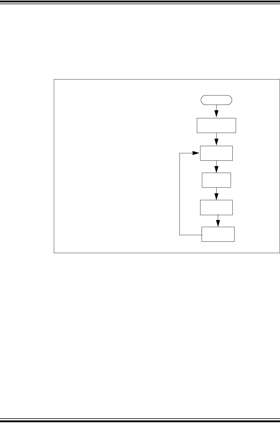
The software flowchart for this lab is shown in Figure 5-6.
FIGURE 5-6: MAIN() SOFTWARE CONTROL LOOP FLOWCHART FOR
ADC LAB 2
The Initialize() configures the peripherals as follows:
•Ports
-Clear PORTB.
- Configure pin 13 as an analog input (using TRISB4).
- Clear the PORTC register.
- Configure RC0 pin as digital output.
•Timer0
- Select the F
OSC/4 internal instruction clock as the Timer0 clock source.
- Increment TMR0 on the low-to-high transition of F
OSC/4.
- Assign the prescaler to Timer0 and configure at a rate of 1:16.
•ADC
- Select ADC conversion clock F
RC
.
- Configure voltage reference using VDD.
- Select channel 10 as the ADC input channel (Pin 13: RB4/AN10).
- Select result format left justified (10-bit result in ADRESH<7:0> and
ADRESL<7:6>).
- Turn on ADC module.
main()
Initialize()
Loop Forever
Get_Inputs()
Decide()
Do_Outputs()
Global variables initialized:
• 8-bit variable TMR0_preload will be used to vary the
delay in Timing() to alter the frequency of the
PWM output on RC0
Timing()