
User manual


Table Of Contents
- Chapter 1. Overview
- 1.1 Introduction
- 1.2 Highlights
- 1.3 PICDEM™ Lab Development Kit Contents
- 1.4 PICDEM™ Lab Development Board Construction and Layout
- 1.5 Target Power
- 1.6 Connecting the PICkit™ 2 Programmer/Debugger
- 1.7 Solderless Prototyping Area Strip Configuration
- Chapter 2. Getting Started
- 2.1 Introduction
- 2.2 Prerequisites
- 2.3 The Software Control Loop
- 2.4 MPLAB® IDE Download Instructions
- 2.5 Installing the Included Lab Files
- Chapter 3. General Purpose Input/Output Labs
- 3.1 Introduction
- 3.2 General Purpose Input/Output Labs
- 3.3 GPIO Output Labs
- 3.3.1 Reference Documentation
- 3.3.2 Equipment Required for GPIO Output Labs
- 3.3.3 PICDEM Lab Development Board Setup for GPIO Output Labs
- Figure 3-1: PICDEM Lab Schematic for GPIO Output Labs
- 3.3.4 Lab 1: Light LEDs
- Figure 3-2: MAIN() Software Control Loop Flowchart for Lab 1
- Figure 3-3: Step One
- Figure 3-4: Step Two
- Figure 3-5: Step Three
- Figure 3-6: Step Four
- Figure 3-7: Summary
- Figure 3-8: Project Window
- Figure 3-9: PICkit 2 PROGRAMMER/DEBUGGER TOOLBAR
- Figure 3-10: Lab 1 LED Output
- 3.3.5 Lab 2: Flash LEDs (Delay Loop)
- Figure 3-11: Main() Software Control Loop Flowchart for Lab 2
- Figure 3-12: Timing() Delay Routine Flowchart for Lab 2
- 3.3.6 Lab 3: Simple Delays Using Timer0
- Equation 3-1: TMR0 Overflow Period using FOSC/4
- Equation 3-2: TMR0 Overflow Period when including the Prescaler
- Equation 3-3: Calculating a TMR0 PreLoad Value to generate a 10mS Overflow Period
- Figure 3-13: Delay_10mS() using Timer0
- Equation 3-4: Maximum TMR0 Overflow Period
- Figure 3-14: Delay_1S() using Timer0
- 3.3.7 Lab 4: Rotate LEDs
- Figure 3-15: Main() Software Control Loop Flowchart for Lab 4
- Figure 3-16: Decide() Flowchart for Lab 4
- Figure 3-17: Results of Do_Output()
- 3.4 GPIO Input Labs
- 3.4.1 Reference Documentation
- 3.4.2 Equipment Required for GPIO Input Labs
- 3.4.3 PICDEM Lab Development Board Setup for GPIO Input Labs
- Figure 3-18: PICDEM Lab Schematic for GPIO Input Labs
- 3.4.4 Lab 5: Adding a Push Button
- Figure 3-19: Main() Software Control Loop Flowchart for Lab 5
- Figure 3-20: Get_Inputs() Software Flowchart for Lab 5
- Figure 3-21: Delay_5mS() Software Flowchart for Lab 5
- Figure 3-22: Decide() Software FlowChart for Lab 5
- 3.4.5 Lab 6: Push Button Interrupt
- Figure 3-23: Main() Software Control Loop Flowchart for GPIO Lab 6
- Figure 3-24: pb_pressISR() for Lab 6 Showing Switch Debounce
- 3.4.6 Lab 7: Push Button Interrupt-on-Change
- Figure 3-25: pb_pressisr Flowchart for Lab 7
- 3.4.7 Lab 8: Using Weak Pull-Ups
- Chapter 4. Comparator Peripheral Labs
- 4.1 Introduction
- 4.2 Comparator Labs
- 4.2.1 Reference Documentation
- 4.2.2 Comparator Labs
- 4.2.3 Equipment Required
- 4.2.4 Lab 1: Simple Compare
- Figure 4-1: Schematic for Comparator Lab 1
- Figure 4-2: Main() software Control Loop Flowchart for Comparator Lab 1
- 4.2.5 Lab 2: Using the Comparator Voltage Reference
- Equation 4-1: CVref Output Voltage
- Equation 4-2: Calculating a 2.5V Internal Reference (Low-Range Method)
- Figure 4-3: Schematic for Comparator Lab 2
- 4.2.6 Lab 3: Higher Resolution Sensor Readings Using a Single Comparator
- Figure 4-4: Basic Relaxation Oscillator Circuit
- Figure 4-5: Schematic for Comparator Lab 3
- Figure 4-6: Main() software Control Loop Flowchart for Comparator Lab 3
- Figure 4-7: TMR0_ISR Flowchart for Comparator Lab 3
- Chapter 5. Analog-to-Digital Converter Peripheral Labs
- 5.1 Introduction
- 5.2 ADC Labs
- Figure 5-1: Schematic for ADC Lab 1
- Figure 5-2: Main() software Control Loop Flowchart for Comparator Lab 1
- Figure 5-3: Main() software Control Loop Flowchart for Comparator Lab 1
- Figure 5-4: ADC Result Bit Significance
- Figure 5-5: Schematic for ADC Lab 2
- Figure 5-6: Main() software Control Loop Flowchart for ADC Lab 2
- Appendix A. Schematic
- Worldwide Sales
General Purpose Input/Output Labs
© 2009 Microchip Technology Inc. DS41369A-page 39
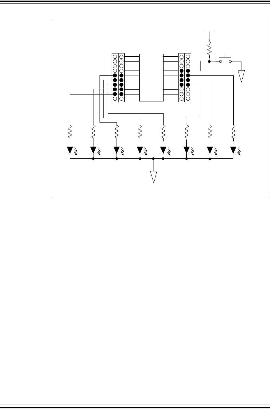
FIGURE 3-18: PICDEM LAB SCHEMATIC FOR GPIO INPUT LABS
The only change from the previous section is the inclusion of a push button connected
to RA2 with associated pull-up resistor.
3.4.4 Lab 5: Adding a Push Button
3.4.4.1 NEW REGISTERS USED IN THIS LAB
To configure the peripherals used in this lab, the following registers are used:
1. PORTA Register: PORTA (Register 4-1 in Section 4 of the PIC16F690 Data
Sheet)
- 8-bit bidirectional port
2. PORTA Tri-State Register: TRISA (Register 4-2 in Section 4 of the PIC16F690
Data Sheet)
- Configures corresponding bits in PORTA as either input or output
3.4.4.2 OVERVIEW
This lab expands upon Lab 4 by adding a push button interface to change the direction
of the sequential shift in the PORTC register.
Mechanical switches play an important and extensive role in practically every
computer, microprocessor and microcontroller application. Mechanical switches are
inexpensive, simple and reliable. However, switches can be very noisy electrically. The
apparent noise is caused by the closing and opening action that seldom results in a
clean electrical transition. The connection makes and breaks several, perhaps even
hundreds, of times before the final switch state settles. The problem is known as switch
bounce. Some of the intermittent activity is due to the switch contacts actually bouncing
off each other. Also, switch contacts are not perfectly smooth. As the contacts move
against each other, the imperfections and impurities on the surfaces cause the
electrical connection to be interrupted. The result is switch bounce. The consequences
U2
1
2
3
4
5
6
7
8
9
10
20
19
18
17
16
15
14
13
12
11
RC0
RC1
RC2
RC3
RC4
RC5
RC6
RC7
J9J8
R8
470Ω
R4
470Ω
R7
470Ω
R6
470Ω
R5
470Ω
R3
470Ω
R2
470Ω
R1
470Ω
LED8 LED7 LED6 LED4 LED3 LED2 LED1LED5
V
SS
V
SS
V
DD
R9
10KΩ
SW1
RA2