
User manual


Table Of Contents
- Chapter 1. Overview
- 1.1 Introduction
- 1.2 Highlights
- 1.3 PICDEM™ Lab Development Kit Contents
- 1.4 PICDEM™ Lab Development Board Construction and Layout
- 1.5 Target Power
- 1.6 Connecting the PICkit™ 2 Programmer/Debugger
- 1.7 Solderless Prototyping Area Strip Configuration
- Chapter 2. Getting Started
- 2.1 Introduction
- 2.2 Prerequisites
- 2.3 The Software Control Loop
- 2.4 MPLAB® IDE Download Instructions
- 2.5 Installing the Included Lab Files
- Chapter 3. General Purpose Input/Output Labs
- 3.1 Introduction
- 3.2 General Purpose Input/Output Labs
- 3.3 GPIO Output Labs
- 3.3.1 Reference Documentation
- 3.3.2 Equipment Required for GPIO Output Labs
- 3.3.3 PICDEM Lab Development Board Setup for GPIO Output Labs
- Figure 3-1: PICDEM Lab Schematic for GPIO Output Labs
- 3.3.4 Lab 1: Light LEDs
- Figure 3-2: MAIN() Software Control Loop Flowchart for Lab 1
- Figure 3-3: Step One
- Figure 3-4: Step Two
- Figure 3-5: Step Three
- Figure 3-6: Step Four
- Figure 3-7: Summary
- Figure 3-8: Project Window
- Figure 3-9: PICkit 2 PROGRAMMER/DEBUGGER TOOLBAR
- Figure 3-10: Lab 1 LED Output
- 3.3.5 Lab 2: Flash LEDs (Delay Loop)
- Figure 3-11: Main() Software Control Loop Flowchart for Lab 2
- Figure 3-12: Timing() Delay Routine Flowchart for Lab 2
- 3.3.6 Lab 3: Simple Delays Using Timer0
- Equation 3-1: TMR0 Overflow Period using FOSC/4
- Equation 3-2: TMR0 Overflow Period when including the Prescaler
- Equation 3-3: Calculating a TMR0 PreLoad Value to generate a 10mS Overflow Period
- Figure 3-13: Delay_10mS() using Timer0
- Equation 3-4: Maximum TMR0 Overflow Period
- Figure 3-14: Delay_1S() using Timer0
- 3.3.7 Lab 4: Rotate LEDs
- Figure 3-15: Main() Software Control Loop Flowchart for Lab 4
- Figure 3-16: Decide() Flowchart for Lab 4
- Figure 3-17: Results of Do_Output()
- 3.4 GPIO Input Labs
- 3.4.1 Reference Documentation
- 3.4.2 Equipment Required for GPIO Input Labs
- 3.4.3 PICDEM Lab Development Board Setup for GPIO Input Labs
- Figure 3-18: PICDEM Lab Schematic for GPIO Input Labs
- 3.4.4 Lab 5: Adding a Push Button
- Figure 3-19: Main() Software Control Loop Flowchart for Lab 5
- Figure 3-20: Get_Inputs() Software Flowchart for Lab 5
- Figure 3-21: Delay_5mS() Software Flowchart for Lab 5
- Figure 3-22: Decide() Software FlowChart for Lab 5
- 3.4.5 Lab 6: Push Button Interrupt
- Figure 3-23: Main() Software Control Loop Flowchart for GPIO Lab 6
- Figure 3-24: pb_pressISR() for Lab 6 Showing Switch Debounce
- 3.4.6 Lab 7: Push Button Interrupt-on-Change
- Figure 3-25: pb_pressisr Flowchart for Lab 7
- 3.4.7 Lab 8: Using Weak Pull-Ups
- Chapter 4. Comparator Peripheral Labs
- 4.1 Introduction
- 4.2 Comparator Labs
- 4.2.1 Reference Documentation
- 4.2.2 Comparator Labs
- 4.2.3 Equipment Required
- 4.2.4 Lab 1: Simple Compare
- Figure 4-1: Schematic for Comparator Lab 1
- Figure 4-2: Main() software Control Loop Flowchart for Comparator Lab 1
- 4.2.5 Lab 2: Using the Comparator Voltage Reference
- Equation 4-1: CVref Output Voltage
- Equation 4-2: Calculating a 2.5V Internal Reference (Low-Range Method)
- Figure 4-3: Schematic for Comparator Lab 2
- 4.2.6 Lab 3: Higher Resolution Sensor Readings Using a Single Comparator
- Figure 4-4: Basic Relaxation Oscillator Circuit
- Figure 4-5: Schematic for Comparator Lab 3
- Figure 4-6: Main() software Control Loop Flowchart for Comparator Lab 3
- Figure 4-7: TMR0_ISR Flowchart for Comparator Lab 3
- Chapter 5. Analog-to-Digital Converter Peripheral Labs
- 5.1 Introduction
- 5.2 ADC Labs
- Figure 5-1: Schematic for ADC Lab 1
- Figure 5-2: Main() software Control Loop Flowchart for Comparator Lab 1
- Figure 5-3: Main() software Control Loop Flowchart for Comparator Lab 1
- Figure 5-4: ADC Result Bit Significance
- Figure 5-5: Schematic for ADC Lab 2
- Figure 5-6: Main() software Control Loop Flowchart for ADC Lab 2
- Appendix A. Schematic
- Worldwide Sales
PICDEM
TM
Lab Development Board User’s Guide
DS41369A-page 26 © 2009 Microchip Technology Inc.
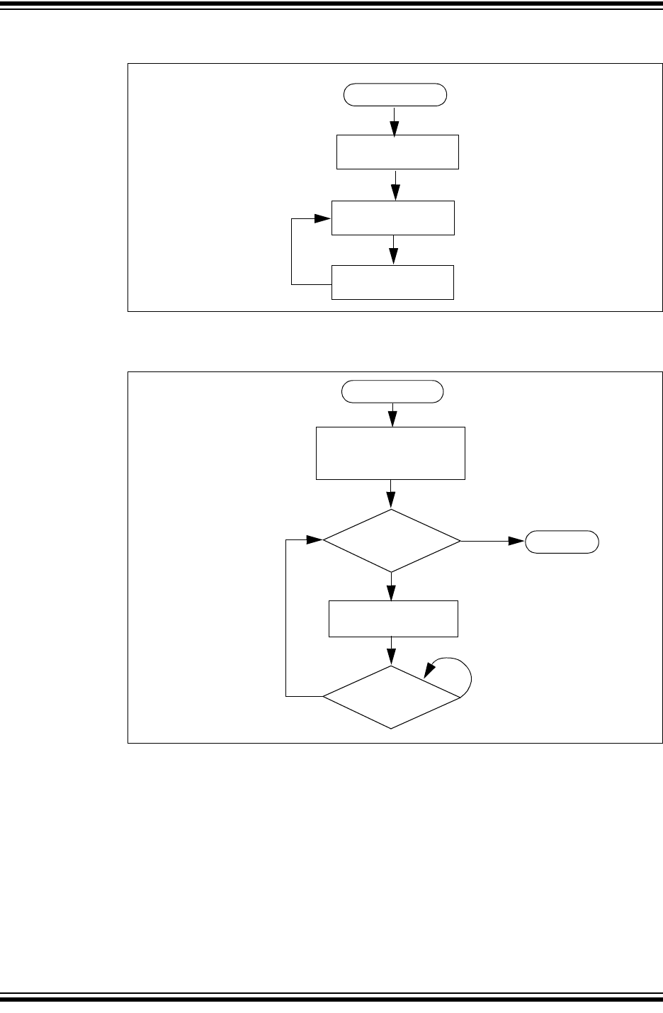
FIGURE 3-11: MAIN() SOFTWARE CONTROL LOOP FLOWCHART FOR
LAB 2
The Timing() delay routine is shown in Figure 3-12.
FIGURE 3-12: TIMING() DELAY ROUTINE FLOWCHART FOR LAB 2
Two variables are used delay_var1 and delay_var2. The delay_var2 is decre-
mented by 1 each time delay_var1 is decremented from 45571 to 0. These values
have been determined through trial and error using a test procedure detailed in the
“Timers: Timer0 Tutorial (Part 1)” (DS51682.pdf) included on the PICDEM™ Lab
Development Kit CD. This delay ties the up the processor for 1 second when using the
4 MHz internal oscillator.
The Initialize() configures the PORTC as follows:
•PORTC
- Set all bits in the PORTC register HIGH
- Configure all PORTC pins as digital outputs
main()
Initialize()
Do_Outputs()
Loop Forever
Timing()
TIMING()
Create two 8-bit variables:
• delay_var1 = 45571
• delay_var2 = 3
delay_var2 - 1 = 0
?
delay_var1 - 1 = 0
?
END
delay_var1 = 45571
YES
YES
NO
NO