
User manual


Table Of Contents
- Chapter 1. Overview
- 1.1 Introduction
- 1.2 Highlights
- 1.3 PICDEM™ Lab Development Kit Contents
- 1.4 PICDEM™ Lab Development Board Construction and Layout
- 1.5 Target Power
- 1.6 Connecting the PICkit™ 2 Programmer/Debugger
- 1.7 Solderless Prototyping Area Strip Configuration
- Chapter 2. Getting Started
- 2.1 Introduction
- 2.2 Prerequisites
- 2.3 The Software Control Loop
- 2.4 MPLAB® IDE Download Instructions
- 2.5 Installing the Included Lab Files
- Chapter 3. General Purpose Input/Output Labs
- 3.1 Introduction
- 3.2 General Purpose Input/Output Labs
- 3.3 GPIO Output Labs
- 3.3.1 Reference Documentation
- 3.3.2 Equipment Required for GPIO Output Labs
- 3.3.3 PICDEM Lab Development Board Setup for GPIO Output Labs
- Figure 3-1: PICDEM Lab Schematic for GPIO Output Labs
- 3.3.4 Lab 1: Light LEDs
- Figure 3-2: MAIN() Software Control Loop Flowchart for Lab 1
- Figure 3-3: Step One
- Figure 3-4: Step Two
- Figure 3-5: Step Three
- Figure 3-6: Step Four
- Figure 3-7: Summary
- Figure 3-8: Project Window
- Figure 3-9: PICkit 2 PROGRAMMER/DEBUGGER TOOLBAR
- Figure 3-10: Lab 1 LED Output
- 3.3.5 Lab 2: Flash LEDs (Delay Loop)
- Figure 3-11: Main() Software Control Loop Flowchart for Lab 2
- Figure 3-12: Timing() Delay Routine Flowchart for Lab 2
- 3.3.6 Lab 3: Simple Delays Using Timer0
- Equation 3-1: TMR0 Overflow Period using FOSC/4
- Equation 3-2: TMR0 Overflow Period when including the Prescaler
- Equation 3-3: Calculating a TMR0 PreLoad Value to generate a 10mS Overflow Period
- Figure 3-13: Delay_10mS() using Timer0
- Equation 3-4: Maximum TMR0 Overflow Period
- Figure 3-14: Delay_1S() using Timer0
- 3.3.7 Lab 4: Rotate LEDs
- Figure 3-15: Main() Software Control Loop Flowchart for Lab 4
- Figure 3-16: Decide() Flowchart for Lab 4
- Figure 3-17: Results of Do_Output()
- 3.4 GPIO Input Labs
- 3.4.1 Reference Documentation
- 3.4.2 Equipment Required for GPIO Input Labs
- 3.4.3 PICDEM Lab Development Board Setup for GPIO Input Labs
- Figure 3-18: PICDEM Lab Schematic for GPIO Input Labs
- 3.4.4 Lab 5: Adding a Push Button
- Figure 3-19: Main() Software Control Loop Flowchart for Lab 5
- Figure 3-20: Get_Inputs() Software Flowchart for Lab 5
- Figure 3-21: Delay_5mS() Software Flowchart for Lab 5
- Figure 3-22: Decide() Software FlowChart for Lab 5
- 3.4.5 Lab 6: Push Button Interrupt
- Figure 3-23: Main() Software Control Loop Flowchart for GPIO Lab 6
- Figure 3-24: pb_pressISR() for Lab 6 Showing Switch Debounce
- 3.4.6 Lab 7: Push Button Interrupt-on-Change
- Figure 3-25: pb_pressisr Flowchart for Lab 7
- 3.4.7 Lab 8: Using Weak Pull-Ups
- Chapter 4. Comparator Peripheral Labs
- 4.1 Introduction
- 4.2 Comparator Labs
- 4.2.1 Reference Documentation
- 4.2.2 Comparator Labs
- 4.2.3 Equipment Required
- 4.2.4 Lab 1: Simple Compare
- Figure 4-1: Schematic for Comparator Lab 1
- Figure 4-2: Main() software Control Loop Flowchart for Comparator Lab 1
- 4.2.5 Lab 2: Using the Comparator Voltage Reference
- Equation 4-1: CVref Output Voltage
- Equation 4-2: Calculating a 2.5V Internal Reference (Low-Range Method)
- Figure 4-3: Schematic for Comparator Lab 2
- 4.2.6 Lab 3: Higher Resolution Sensor Readings Using a Single Comparator
- Figure 4-4: Basic Relaxation Oscillator Circuit
- Figure 4-5: Schematic for Comparator Lab 3
- Figure 4-6: Main() software Control Loop Flowchart for Comparator Lab 3
- Figure 4-7: TMR0_ISR Flowchart for Comparator Lab 3
- Chapter 5. Analog-to-Digital Converter Peripheral Labs
- 5.1 Introduction
- 5.2 ADC Labs
- Figure 5-1: Schematic for ADC Lab 1
- Figure 5-2: Main() software Control Loop Flowchart for Comparator Lab 1
- Figure 5-3: Main() software Control Loop Flowchart for Comparator Lab 1
- Figure 5-4: ADC Result Bit Significance
- Figure 5-5: Schematic for ADC Lab 2
- Figure 5-6: Main() software Control Loop Flowchart for ADC Lab 2
- Appendix A. Schematic
- Worldwide Sales
PICDEM
TM
Lab Development Board User’s Guide
DS41369A-page 18 © 2009 Microchip Technology Inc.
3.3 GPIO OUTPUT LABS
3.3.1 Reference Documentation
All documentation is available on the PICDEM™ Lab Development Kit accompanying
CD-ROM.
• PIC16F690 Data Sheet (DS41262)
- Section 2.2.2.2: Option Register
- Section 2.2.2.3: Interrupt Control Register INTCON
- Section 4: I/O Ports
- Section 5: Timer0 Module
• Timers: Timer0 Tutorial (Part 1) (DS51628)
• Timers: Timer0 Tutorial (Part 2) (DS51702)
• “Introduction to MPLAB
®
IDE and HI-TECH C
®
PRO for the PIC10/12/16 MCU
Family Lite Mode Compiler Tutorial” (DS41322)
3.3.2 Equipment Required for GPIO Output Labs
To complete the labs in this section, the following components are required:
1. 8 – Light Emitting Diodes
2. 8 – 470Ω resistors
3. PIC16F690 populating socket U2
4. Assorted jumper wires
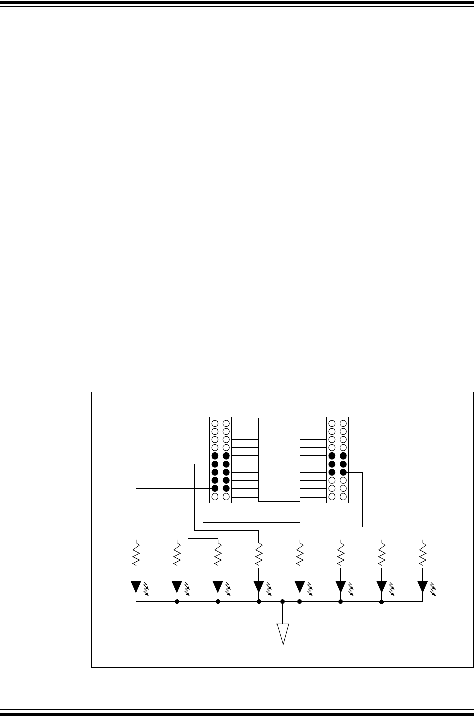
3.3.3 PICDEM Lab Development Board Setup for GPIO Output Labs
The GPIO output labs will require that the PICDEM Lab Development Board be config-
ured as shown in Figure 3-1 using the components listed in the previous section.
FIGURE 3-1: PICDEM LAB SCHEMATIC FOR GPIO OUTPUT LABS
U2
1
2
3
4
5
6
7
8
9
10
20
19
18
17
16
15
14
13
12
11
RC0
RC1
RC2
RC3
RC4
RC5
RC6
RC7
J9J8
R8
470Ω
R4
470Ω
R7
470Ω
R6
470Ω
R5
470Ω
R3
470Ω
R2
470Ω
R1
470Ω
LED8 LED7 LED6 LED4 LED3 LED2 LED1LED5
V
SS