
User manual


Table Of Contents
- Chapter 1. Overview
- 1.1 Introduction
- 1.2 Highlights
- 1.3 PICDEM™ Lab Development Kit Contents
- 1.4 PICDEM™ Lab Development Board Construction and Layout
- 1.5 Target Power
- 1.6 Connecting the PICkit™ 2 Programmer/Debugger
- 1.7 Solderless Prototyping Area Strip Configuration
- Chapter 2. Getting Started
- 2.1 Introduction
- 2.2 Prerequisites
- 2.3 The Software Control Loop
- 2.4 MPLAB® IDE Download Instructions
- 2.5 Installing the Included Lab Files
- Chapter 3. General Purpose Input/Output Labs
- 3.1 Introduction
- 3.2 General Purpose Input/Output Labs
- 3.3 GPIO Output Labs
- 3.3.1 Reference Documentation
- 3.3.2 Equipment Required for GPIO Output Labs
- 3.3.3 PICDEM Lab Development Board Setup for GPIO Output Labs
- Figure 3-1: PICDEM Lab Schematic for GPIO Output Labs
- 3.3.4 Lab 1: Light LEDs
- Figure 3-2: MAIN() Software Control Loop Flowchart for Lab 1
- Figure 3-3: Step One
- Figure 3-4: Step Two
- Figure 3-5: Step Three
- Figure 3-6: Step Four
- Figure 3-7: Summary
- Figure 3-8: Project Window
- Figure 3-9: PICkit 2 PROGRAMMER/DEBUGGER TOOLBAR
- Figure 3-10: Lab 1 LED Output
- 3.3.5 Lab 2: Flash LEDs (Delay Loop)
- Figure 3-11: Main() Software Control Loop Flowchart for Lab 2
- Figure 3-12: Timing() Delay Routine Flowchart for Lab 2
- 3.3.6 Lab 3: Simple Delays Using Timer0
- Equation 3-1: TMR0 Overflow Period using FOSC/4
- Equation 3-2: TMR0 Overflow Period when including the Prescaler
- Equation 3-3: Calculating a TMR0 PreLoad Value to generate a 10mS Overflow Period
- Figure 3-13: Delay_10mS() using Timer0
- Equation 3-4: Maximum TMR0 Overflow Period
- Figure 3-14: Delay_1S() using Timer0
- 3.3.7 Lab 4: Rotate LEDs
- Figure 3-15: Main() Software Control Loop Flowchart for Lab 4
- Figure 3-16: Decide() Flowchart for Lab 4
- Figure 3-17: Results of Do_Output()
- 3.4 GPIO Input Labs
- 3.4.1 Reference Documentation
- 3.4.2 Equipment Required for GPIO Input Labs
- 3.4.3 PICDEM Lab Development Board Setup for GPIO Input Labs
- Figure 3-18: PICDEM Lab Schematic for GPIO Input Labs
- 3.4.4 Lab 5: Adding a Push Button
- Figure 3-19: Main() Software Control Loop Flowchart for Lab 5
- Figure 3-20: Get_Inputs() Software Flowchart for Lab 5
- Figure 3-21: Delay_5mS() Software Flowchart for Lab 5
- Figure 3-22: Decide() Software FlowChart for Lab 5
- 3.4.5 Lab 6: Push Button Interrupt
- Figure 3-23: Main() Software Control Loop Flowchart for GPIO Lab 6
- Figure 3-24: pb_pressISR() for Lab 6 Showing Switch Debounce
- 3.4.6 Lab 7: Push Button Interrupt-on-Change
- Figure 3-25: pb_pressisr Flowchart for Lab 7
- 3.4.7 Lab 8: Using Weak Pull-Ups
- Chapter 4. Comparator Peripheral Labs
- 4.1 Introduction
- 4.2 Comparator Labs
- 4.2.1 Reference Documentation
- 4.2.2 Comparator Labs
- 4.2.3 Equipment Required
- 4.2.4 Lab 1: Simple Compare
- Figure 4-1: Schematic for Comparator Lab 1
- Figure 4-2: Main() software Control Loop Flowchart for Comparator Lab 1
- 4.2.5 Lab 2: Using the Comparator Voltage Reference
- Equation 4-1: CVref Output Voltage
- Equation 4-2: Calculating a 2.5V Internal Reference (Low-Range Method)
- Figure 4-3: Schematic for Comparator Lab 2
- 4.2.6 Lab 3: Higher Resolution Sensor Readings Using a Single Comparator
- Figure 4-4: Basic Relaxation Oscillator Circuit
- Figure 4-5: Schematic for Comparator Lab 3
- Figure 4-6: Main() software Control Loop Flowchart for Comparator Lab 3
- Figure 4-7: TMR0_ISR Flowchart for Comparator Lab 3
- Chapter 5. Analog-to-Digital Converter Peripheral Labs
- 5.1 Introduction
- 5.2 ADC Labs
- Figure 5-1: Schematic for ADC Lab 1
- Figure 5-2: Main() software Control Loop Flowchart for Comparator Lab 1
- Figure 5-3: Main() software Control Loop Flowchart for Comparator Lab 1
- Figure 5-4: ADC Result Bit Significance
- Figure 5-5: Schematic for ADC Lab 2
- Figure 5-6: Main() software Control Loop Flowchart for ADC Lab 2
- Appendix A. Schematic
- Worldwide Sales
PICDEM
TM
LAB DEVELOPMENT
BOARD USER’S GUIDE
© 2009 Microchip Technology Inc. SD41369A-page 11
Chapter 2. Getting Started
2.1 INTRODUCTION
This chapter is intended to prepare the reader to complete the labs in the remaining
chapters of this user’s guide.
2.2 PREREQUISITES
The labs contained within this lab manual assumes the user:
1. Has a basic understanding of the C programming language.
2. Understands basic circuit analysis.
3. Has completed or understands the concepts contained within the introductory
tutorial: “Introduction to MPLAB
®
IDE and HI-TECH C
®
PRO for the PIC10/12/16
MCU Family Lite Mode Compiler Tutorial” (DS41322B) provided on the
accompanying CD-ROM.
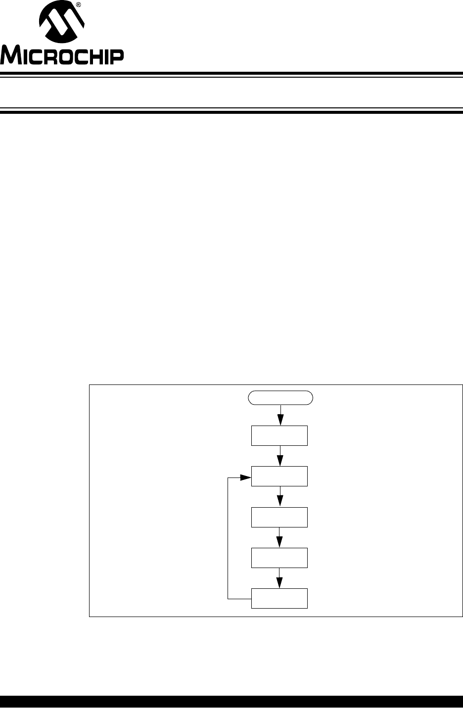
2.3 THE SOFTWARE CONTROL LOOP
The labs used in this user’s guide implement a software control loop in various
configurations but always in the same sequence as shown in Example 2-1.
FIGURE 2-1: MAIN() SOFTWARE CONTROL LOOP FLOWCHART FOR
USED IN LABS
Each block of the software control loop represents a function that organizes tasks into
logical, organized groupings that are called from the main function (main()). Notice
the Initialize() is called only once while the remaining functions are executed
repeatedly. This method organizes the embedded firmware application into a logic
sequence of events:
main()
Loop Forever
Timing()
Initialize()
Get_Inputs()
Decide()
Do_Outputs()