
User manual


Table Of Contents
- Chapter 1. Introduction
- Chapter 2. Getting Started
- Chapter 3. Using the Demo Software
- Appendix A. Board Technical Information
- Figure A-1: PICDEM™ LCD 2 Default Jumper Location
- A.1 Processors
- A.2 LCD Display
- Figure A-2: PICDEM™ LCD 2 Display
- Table A-2: LCD Glass Specifications
- Figure A-3: Display Definitions
- Figure A-4: Digit Description
- Table A-3: LCD SEGx and COMx
- A.2.1 Device-Specific LCD Segment Configuration
- Table A-4: PIC18F85J90 PIM and ICE Pin/Port Comparison
- Table A-5: PIC18F85J90 LCD connections Comparison
- Figure A-5: Segment Configuration for PIC18F85J90 Devices
- Table A-6: PIC18F85j90 pORT AND pIN cOMPARISON
- Table A-7: PIC18F87J90 PIM and ICE Pin/Port Comparison
- Table A-8: PIC18F87J90 LCD connections Comparison
- Figure A-6: Segment Configuration for PIC18F87J90 Devices
- Table A-9: PIC18F87j90 pORT AND pIN cOMPARISON
- Table A-10: PIC18F8490 Pim and ICE Port/Pin Comparison
- Table A-11: pic18f8490 LCD cONNECTIONS cOMPARISON
- Figure A-7: Segment Configuration for PIC18F8490 Devices
- Table A-12: pic18f8490 pIN AND pORT cOMPARISON
- Table A-13: PIC16F946 PIM and ICE PIn/Port Comparison
- Table A-14: PIC16F946 LCD Connections cOMPARISON
- Figure A-8: Segment Configuration for PIC16F946 Devices
- Table A-15: pic16f946 pORT AND PIN cOMPARISON
- Table A-16: PIC16F/LF1946/7 PIM and ICE PIn/Port Comparison
- Table A-17: PIC16F/LF1946/7 LCD Connections cOMPARISON
- Figure A-9: Segment Configuration for PIC16F/LF1946/7 Devices
- Table A-18: pic16f/LF1946/7 pORT AND PIN cOMPARISON
- Table A-19: PIC16F917 PIM and ICE Pin/Port Comparison
- Table A-20: pic16f917 LCD cONNECTIONS cOMPARISON
- Figure A-10: Segment Configuration for PIC16F914/917 Devices
- Table A-21: pic16f917 pIN AND pORT cOMPARISON
- A.3 LED Display
- A.4 Charge Pump and VLCAP
- A.5 Resistive Ladder Versus Charge Pump
- A.6 Oscillator Options
- A.7 RS-232 Serial Port
- A.8 Real-Time Clock
- A.9 Serial EEPROM
- A.10 Analog Input
- A.11 Temperature Sensor
- A.12 Switches
- A.13 ICD Connector
- A.14 Power Supply
- A.15 Board Layout and Schematics
- A.16 PIM Layout and Schematics
- Figure A-16: PIC18F65J90 and PIC18F85J90 PIM Layout
- Figure A-17: PIC16F914/917 PIM Layout
- Figure A-18: PIC16F946 PIM Layout
- Figure A-19: PIC16F/LF1946/7 PIM Layout
- Figure A-20: PIC18F6490/8490 PIM Layout
- Figure A-21: PIC18F87j90 PIM Layout
- Figure A-22: PICDEM™ LCD 2 PIC16F914/917 PIM Schematic
- Figure A-23: PICDEM LCD 2 PIC16F/LF1946/7 64-Pin PIM Schematic
- Figure A-24: PICDEM™ LCD 2 PIC16F946 PIM Schematic
- Figure A-25: PICDEM™ LCD 2 PIC18F6490 64-pin PIM Schematic
- Figure A-26: PICDEM™ LCD 2 PIC18F8490 80-pin PIM Schematic
- Figure A-27: PICDEM™ LCD 2 PIC18F6XJ90 64-pin PIM Schematic
- Figure A-28: PICDEM™ LCD 2 PIC18F87J90 80-pin PIM Schematic
- Figure A-29: PICDEM™ LCD 2 PIC18F85J90 80-pin PIM Schematic
- Worldwide Sales and Service
Board Technical Information
2010 Microchip Technology Inc. DS51662C-page 51
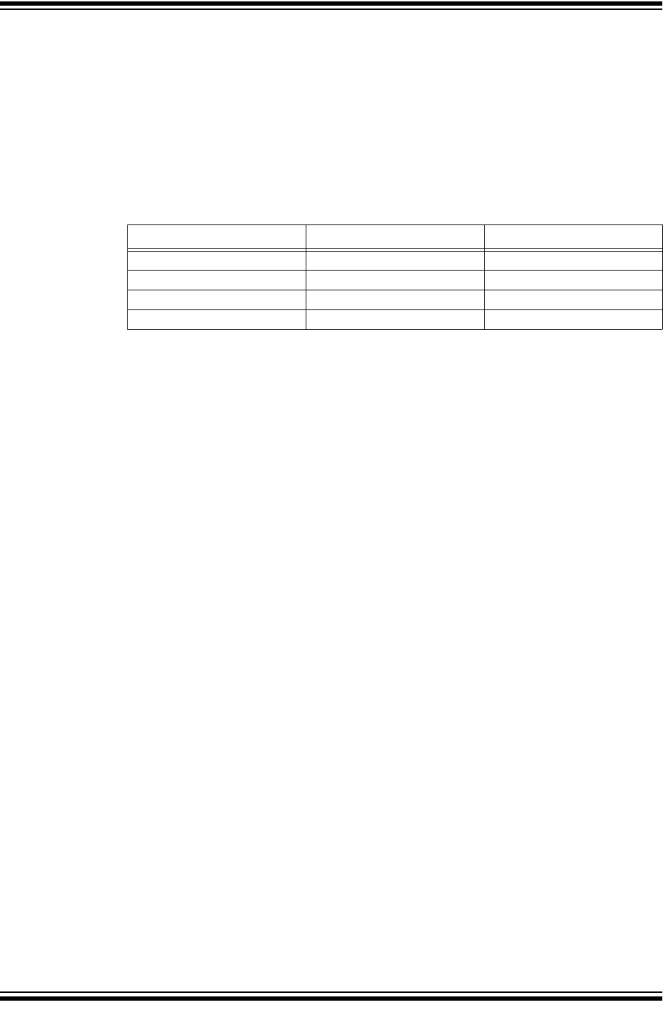
As stated previously, R25 = 1K and R26 = 330. You can see that without R102 and
R101, V
OUT = 1.25V(1+ 1K/330R) = 5.04V.
For a desired V
OUT, first solve for R2, given R1 = R26 = 330R. Then, knowing R2 and
R25, solve for R102. Determine the nearest available resistor value for R102 and
recalculate the resulting V
DD to make sure it does not exceed the maximum VDD for the
part you will be using.
Table A-23 shows values for R101 and R102 for different V
DD values, assuming that
R25 and R26 on the PICDEM LCD 2 Board are left as their default values of 1K and
330R.
Recommended operating voltages for the various PIMs are:
• PIC18F85J90 and PIC18F87J90 families of devices – 3.3V
• PIC18F8490 family of devices – 5V
• PIC16F917/914 devices – 5V
• PIC16F946 – 5V (when operating on an external 9V DC supply)
• PIC16F1946/7 – 5V
• PIC16LF1946/7 – 3.3V
A.14.2 Slide Switch (S6)
The slide switch allows choosing the BIAS values, either generated by the resistor
ladder, or by the capacitive charge pump. When S6 is switched to the left, the LCDBIAS
pins of the microcontroller are connected to the resistor ladder. When S6 is switched to
the right, the LCDBIAS pins of the microcontroller are connected to the capacitor
network.
TABLE A-23: R101 AND R102 V
DD VALUES
VDD R101 R102
5V Open Open
3.6V Open 1.62K
3.3V Open 1.18K
3.0V Open 866R