
User manual


Table Of Contents
- Chapter 1. Introduction
- Chapter 2. Getting Started
- Chapter 3. Using the Demo Software
- Appendix A. Board Technical Information
- Figure A-1: PICDEM™ LCD 2 Default Jumper Location
- A.1 Processors
- A.2 LCD Display
- Figure A-2: PICDEM™ LCD 2 Display
- Table A-2: LCD Glass Specifications
- Figure A-3: Display Definitions
- Figure A-4: Digit Description
- Table A-3: LCD SEGx and COMx
- A.2.1 Device-Specific LCD Segment Configuration
- Table A-4: PIC18F85J90 PIM and ICE Pin/Port Comparison
- Table A-5: PIC18F85J90 LCD connections Comparison
- Figure A-5: Segment Configuration for PIC18F85J90 Devices
- Table A-6: PIC18F85j90 pORT AND pIN cOMPARISON
- Table A-7: PIC18F87J90 PIM and ICE Pin/Port Comparison
- Table A-8: PIC18F87J90 LCD connections Comparison
- Figure A-6: Segment Configuration for PIC18F87J90 Devices
- Table A-9: PIC18F87j90 pORT AND pIN cOMPARISON
- Table A-10: PIC18F8490 Pim and ICE Port/Pin Comparison
- Table A-11: pic18f8490 LCD cONNECTIONS cOMPARISON
- Figure A-7: Segment Configuration for PIC18F8490 Devices
- Table A-12: pic18f8490 pIN AND pORT cOMPARISON
- Table A-13: PIC16F946 PIM and ICE PIn/Port Comparison
- Table A-14: PIC16F946 LCD Connections cOMPARISON
- Figure A-8: Segment Configuration for PIC16F946 Devices
- Table A-15: pic16f946 pORT AND PIN cOMPARISON
- Table A-16: PIC16F/LF1946/7 PIM and ICE PIn/Port Comparison
- Table A-17: PIC16F/LF1946/7 LCD Connections cOMPARISON
- Figure A-9: Segment Configuration for PIC16F/LF1946/7 Devices
- Table A-18: pic16f/LF1946/7 pORT AND PIN cOMPARISON
- Table A-19: PIC16F917 PIM and ICE Pin/Port Comparison
- Table A-20: pic16f917 LCD cONNECTIONS cOMPARISON
- Figure A-10: Segment Configuration for PIC16F914/917 Devices
- Table A-21: pic16f917 pIN AND pORT cOMPARISON
- A.3 LED Display
- A.4 Charge Pump and VLCAP
- A.5 Resistive Ladder Versus Charge Pump
- A.6 Oscillator Options
- A.7 RS-232 Serial Port
- A.8 Real-Time Clock
- A.9 Serial EEPROM
- A.10 Analog Input
- A.11 Temperature Sensor
- A.12 Switches
- A.13 ICD Connector
- A.14 Power Supply
- A.15 Board Layout and Schematics
- A.16 PIM Layout and Schematics
- Figure A-16: PIC18F65J90 and PIC18F85J90 PIM Layout
- Figure A-17: PIC16F914/917 PIM Layout
- Figure A-18: PIC16F946 PIM Layout
- Figure A-19: PIC16F/LF1946/7 PIM Layout
- Figure A-20: PIC18F6490/8490 PIM Layout
- Figure A-21: PIC18F87j90 PIM Layout
- Figure A-22: PICDEM™ LCD 2 PIC16F914/917 PIM Schematic
- Figure A-23: PICDEM LCD 2 PIC16F/LF1946/7 64-Pin PIM Schematic
- Figure A-24: PICDEM™ LCD 2 PIC16F946 PIM Schematic
- Figure A-25: PICDEM™ LCD 2 PIC18F6490 64-pin PIM Schematic
- Figure A-26: PICDEM™ LCD 2 PIC18F8490 80-pin PIM Schematic
- Figure A-27: PICDEM™ LCD 2 PIC18F6XJ90 64-pin PIM Schematic
- Figure A-28: PICDEM™ LCD 2 PIC18F87J90 80-pin PIM Schematic
- Figure A-29: PICDEM™ LCD 2 PIC18F85J90 80-pin PIM Schematic
- Worldwide Sales and Service
PICDEM™ LCD 2 Demonstration Kit User’s Guide
DS51662C-page 50 2010 Microchip Technology Inc.
A.14.1 Using the Adjustable Voltage Regulator
The PICDEM LCD 2 board features an adjustable voltage regulator, the venerable
LM317. It is U3 on the board, and can be recognized by the SO-223 package on the
upper left side. Nearby, there is a header, J10, and two resistors, R25 and R26. R25
and R26 are used to set the output voltage of the LM317. By default, R25 = 1K and
R26 = 330R, which results in an output voltage of 5.0V.
The reason an adjustable voltage regulator is provided is so that the PICDEM LCD 2
Demonstration Board can be used with a wide range of LCD PIC microcontrollers. The
PIC18FXXJ90 family of devices tolerates a maximum V
DD of 3.6V, whereas the
PIC18FXX90, PIC16F91X and PIC16F946 tolerate a maximum V
DD of 5.5V. The
adjustable voltage regulator allows a different V
DD to be provided for PIC18FJ devices
and PIC18F and PIC16F LCD devices.
The switching between 3.6V and 5.5V parts is very convenient. The plug-in module
boards are populated with the R101 and R102, appropriately, according to the proces-
sor module requirement which mates with the daughter board/emulator header that
surrounds the ICE module (U1A). J10 on the PICDEM LCD 2 board is intended to con-
nect with the 3-pin header on the plug-in module. This allows the resistors, R101 and
R102, on the plug-in module to be connected in parallel to the resistors, R25 and R26.
This way V
DD can automatically be adjusted to the voltage appropriate to the part
soldered onto the plug-in module.
The plug-in module is prepopulated with the values shown in Table A-22:
For V
DD = 3.3 volts, R101 can be left unpopulated and R102 can be 1.18K.
(1% resistors are recommended for precise adjustment of V
DD.)
Now, let’s look at how to determine R101 and R102 if a different V
DD is desired. First,
it is a good idea to look at the data sheet for the LM317 to understand how the voltage
is adjusted. We will not duplicate all the details here. The following equation is taken
from an LM317 data sheet:
EQUATION A-1:
I
ADJ is minimized by the LM317, so it can be assumed to be zero or at least very small.
V
REF =1.25V; it is the reference voltage developed by the LM317 between the output
and adjustment terminal.
That gives us the following equation:
EQUATION A-2:
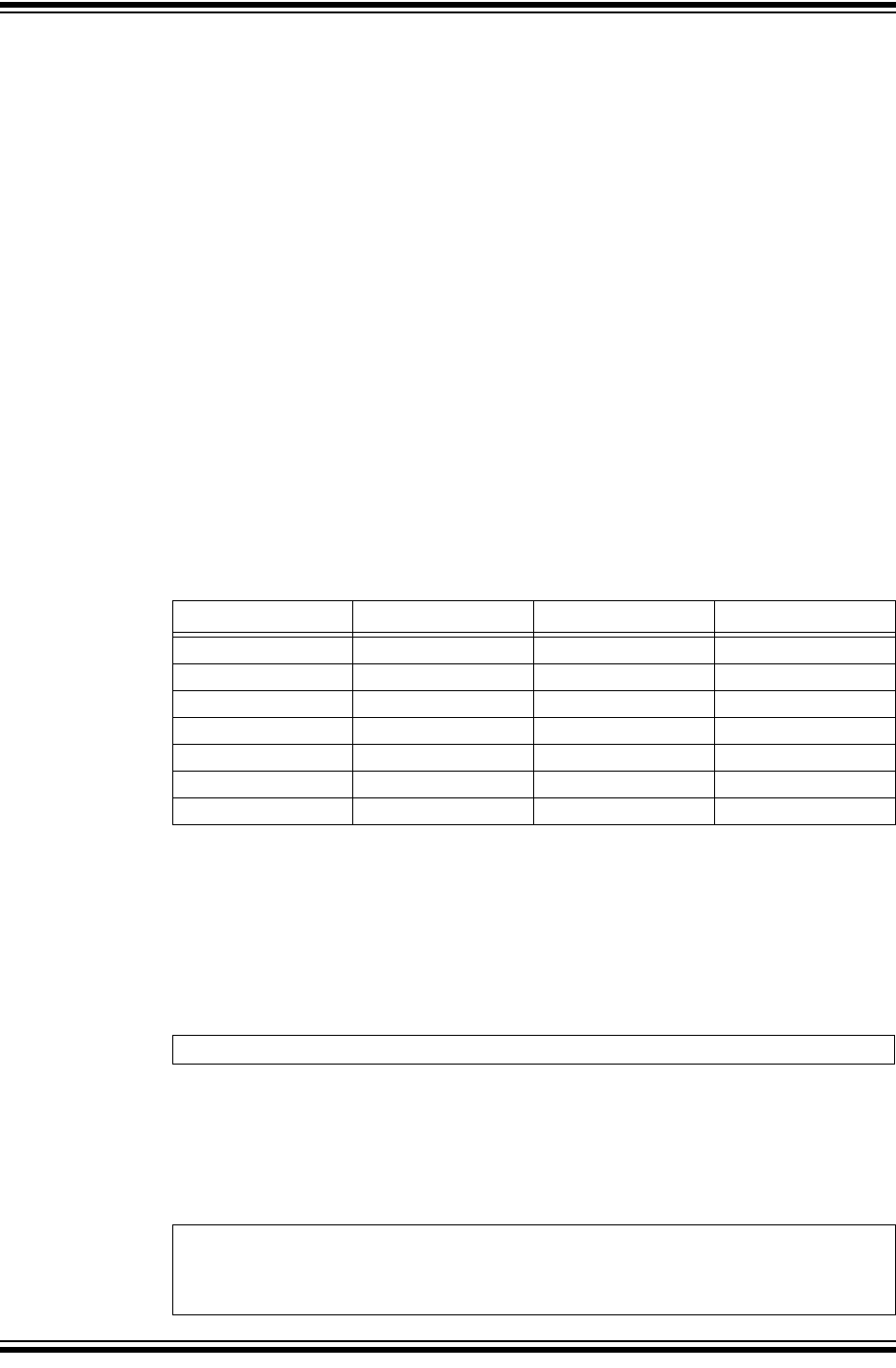
TABLE A-22: PIM PREPOPULATED VALUES
Module R101 R102 VDD
PIC18F87J90 Open 1.18K 3.3V
PIC18F85J90 Open 1.18K 3.3V
PIC18F8490 Open Open 5.0V
PIC16F914/917 Open Open 5.0V
PIC16F946 Open Open 5.0V
PIC16F1946/7 Open Open 5.0V
PIC16LF1946/7 Open 1.18K 3.3V
VOUT = VREF (1+ R2/R1) + IADJ * R2
VOUT = 1.25V(1+R2/R1)
R2 = R25 || R102 = (R25* R102)/(R25+R102)
R1 = R26 || R101.= (R26* R101)/(R26+R101)