
User manual


Table Of Contents
- Chapter 1. Introduction
- Chapter 2. Getting Started
- Chapter 3. Using the Demo Software
- Appendix A. Board Technical Information
- Figure A-1: PICDEM™ LCD 2 Default Jumper Location
- A.1 Processors
- A.2 LCD Display
- Figure A-2: PICDEM™ LCD 2 Display
- Table A-2: LCD Glass Specifications
- Figure A-3: Display Definitions
- Figure A-4: Digit Description
- Table A-3: LCD SEGx and COMx
- A.2.1 Device-Specific LCD Segment Configuration
- Table A-4: PIC18F85J90 PIM and ICE Pin/Port Comparison
- Table A-5: PIC18F85J90 LCD connections Comparison
- Figure A-5: Segment Configuration for PIC18F85J90 Devices
- Table A-6: PIC18F85j90 pORT AND pIN cOMPARISON
- Table A-7: PIC18F87J90 PIM and ICE Pin/Port Comparison
- Table A-8: PIC18F87J90 LCD connections Comparison
- Figure A-6: Segment Configuration for PIC18F87J90 Devices
- Table A-9: PIC18F87j90 pORT AND pIN cOMPARISON
- Table A-10: PIC18F8490 Pim and ICE Port/Pin Comparison
- Table A-11: pic18f8490 LCD cONNECTIONS cOMPARISON
- Figure A-7: Segment Configuration for PIC18F8490 Devices
- Table A-12: pic18f8490 pIN AND pORT cOMPARISON
- Table A-13: PIC16F946 PIM and ICE PIn/Port Comparison
- Table A-14: PIC16F946 LCD Connections cOMPARISON
- Figure A-8: Segment Configuration for PIC16F946 Devices
- Table A-15: pic16f946 pORT AND PIN cOMPARISON
- Table A-16: PIC16F/LF1946/7 PIM and ICE PIn/Port Comparison
- Table A-17: PIC16F/LF1946/7 LCD Connections cOMPARISON
- Figure A-9: Segment Configuration for PIC16F/LF1946/7 Devices
- Table A-18: pic16f/LF1946/7 pORT AND PIN cOMPARISON
- Table A-19: PIC16F917 PIM and ICE Pin/Port Comparison
- Table A-20: pic16f917 LCD cONNECTIONS cOMPARISON
- Figure A-10: Segment Configuration for PIC16F914/917 Devices
- Table A-21: pic16f917 pIN AND pORT cOMPARISON
- A.3 LED Display
- A.4 Charge Pump and VLCAP
- A.5 Resistive Ladder Versus Charge Pump
- A.6 Oscillator Options
- A.7 RS-232 Serial Port
- A.8 Real-Time Clock
- A.9 Serial EEPROM
- A.10 Analog Input
- A.11 Temperature Sensor
- A.12 Switches
- A.13 ICD Connector
- A.14 Power Supply
- A.15 Board Layout and Schematics
- A.16 PIM Layout and Schematics
- Figure A-16: PIC18F65J90 and PIC18F85J90 PIM Layout
- Figure A-17: PIC16F914/917 PIM Layout
- Figure A-18: PIC16F946 PIM Layout
- Figure A-19: PIC16F/LF1946/7 PIM Layout
- Figure A-20: PIC18F6490/8490 PIM Layout
- Figure A-21: PIC18F87j90 PIM Layout
- Figure A-22: PICDEM™ LCD 2 PIC16F914/917 PIM Schematic
- Figure A-23: PICDEM LCD 2 PIC16F/LF1946/7 64-Pin PIM Schematic
- Figure A-24: PICDEM™ LCD 2 PIC16F946 PIM Schematic
- Figure A-25: PICDEM™ LCD 2 PIC18F6490 64-pin PIM Schematic
- Figure A-26: PICDEM™ LCD 2 PIC18F8490 80-pin PIM Schematic
- Figure A-27: PICDEM™ LCD 2 PIC18F6XJ90 64-pin PIM Schematic
- Figure A-28: PICDEM™ LCD 2 PIC18F87J90 80-pin PIM Schematic
- Figure A-29: PICDEM™ LCD 2 PIC18F85J90 80-pin PIM Schematic
- Worldwide Sales and Service
Board Technical Information
2010 Microchip Technology Inc. DS51662C-page 49
A.14 POWER SUPPLY
There are four ways to supply power to the PICDEM LCD 2:
• A 3V button cell (CR2032) can be plugged into BT1.
• A 9V, 100 mA unregulated AC to DC supply can be plugged into J5. A
power supply can be purchased through Microchip Technology
(Part Number AC162039).
• A 100 mA regulated DC supply of maximum +5V can be connected to the hooks
provided.
MPLAB ICD 2 users may use the ICD to power the target board to 5V, up to 200 mA,
for the following devices only: PIC18F8490, PIC16F/LF/1946/7, PIC16F946 and
PIC16F916. The PIC18F85J90 and PIC18F87J90 families of devices do not support
this capability.
The default power on the board is 5V. The board voltage can be varied based on
resistors populated on the PIM in conjunction with the processor being used.
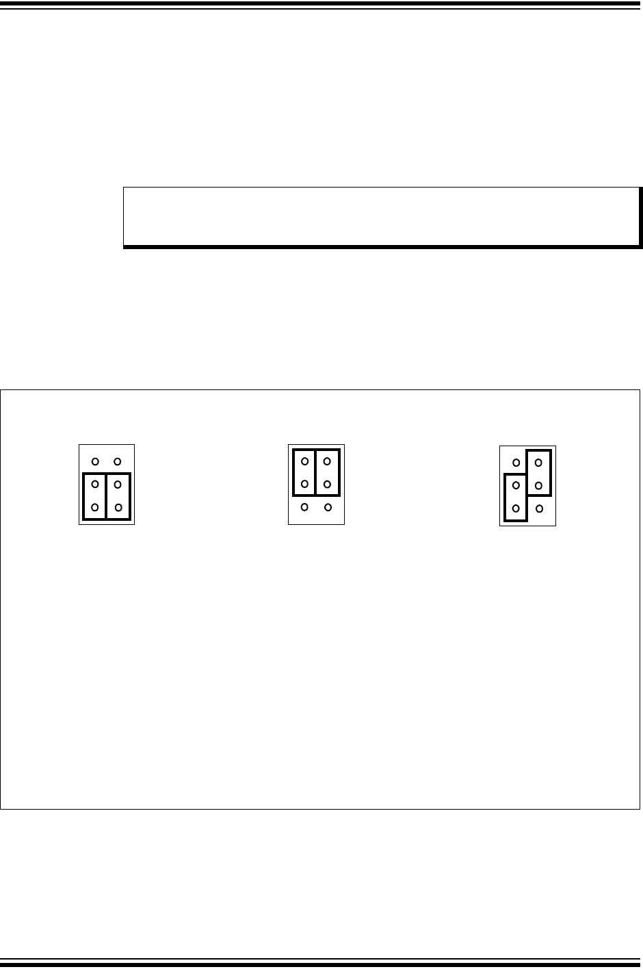
FIGURE A-11: J15 POWER SUPPLY CIRCUIT SETTING EXAMPLES
Note: There is one J15 jumper associated with the power supply circuit. This
jumper must be correctly connected to select the required power supply.
Refer to Figure A-11 for jumper setting examples.
1
3
5
2
4
6
J15
VLCDBIAS = Battery
1
3
5
2
4
6
J15
1
3
5
2
4
6
J15
VLCDBIAS = VCC
a) External Supply with
VLCDBIAS Regulated
(Default): This is the recom-
mended jumper setting to
operate when using external
supply. This configuration
allows the VLCDBIAS to be
regulated to 3V even if the V
DD
of the board is higher than 3V.
VLCDBIAS = 3V, External Power
b) Battery Operation: This is the
recommend jumper setting
when operating on a battery. In
this configuration, VLCDBIAS is
directly connected to the battery
voltage.
c) External Supply with VLCDBIAS
Unregulated: This is not recom-
mended to use with on-board glass
as voltage higher than 3V may
damage the glass.
If an external glass is connected to
J2 and is capable of handling
higher voltages, then this jumper
setting allows V
CC to connect
directly to the VLCDBIAS when an
external power supply is used.
EXAMPLE A EXAMPLE B EXAMPLE C
Note: For all examples shown above, the voltage regulation on the VLCDBIAS for 3V is not required for the
regular operation of the module or device. It is added here for additional protection for the glass since
the board is capable of generating 3.3V or 5V depending on the PIM being used.