
User manual


Table Of Contents
- Chapter 1. Introduction
- Chapter 2. Getting Started
- Chapter 3. Using the Demo Software
- Appendix A. Board Technical Information
- Figure A-1: PICDEM™ LCD 2 Default Jumper Location
- A.1 Processors
- A.2 LCD Display
- Figure A-2: PICDEM™ LCD 2 Display
- Table A-2: LCD Glass Specifications
- Figure A-3: Display Definitions
- Figure A-4: Digit Description
- Table A-3: LCD SEGx and COMx
- A.2.1 Device-Specific LCD Segment Configuration
- Table A-4: PIC18F85J90 PIM and ICE Pin/Port Comparison
- Table A-5: PIC18F85J90 LCD connections Comparison
- Figure A-5: Segment Configuration for PIC18F85J90 Devices
- Table A-6: PIC18F85j90 pORT AND pIN cOMPARISON
- Table A-7: PIC18F87J90 PIM and ICE Pin/Port Comparison
- Table A-8: PIC18F87J90 LCD connections Comparison
- Figure A-6: Segment Configuration for PIC18F87J90 Devices
- Table A-9: PIC18F87j90 pORT AND pIN cOMPARISON
- Table A-10: PIC18F8490 Pim and ICE Port/Pin Comparison
- Table A-11: pic18f8490 LCD cONNECTIONS cOMPARISON
- Figure A-7: Segment Configuration for PIC18F8490 Devices
- Table A-12: pic18f8490 pIN AND pORT cOMPARISON
- Table A-13: PIC16F946 PIM and ICE PIn/Port Comparison
- Table A-14: PIC16F946 LCD Connections cOMPARISON
- Figure A-8: Segment Configuration for PIC16F946 Devices
- Table A-15: pic16f946 pORT AND PIN cOMPARISON
- Table A-16: PIC16F/LF1946/7 PIM and ICE PIn/Port Comparison
- Table A-17: PIC16F/LF1946/7 LCD Connections cOMPARISON
- Figure A-9: Segment Configuration for PIC16F/LF1946/7 Devices
- Table A-18: pic16f/LF1946/7 pORT AND PIN cOMPARISON
- Table A-19: PIC16F917 PIM and ICE Pin/Port Comparison
- Table A-20: pic16f917 LCD cONNECTIONS cOMPARISON
- Figure A-10: Segment Configuration for PIC16F914/917 Devices
- Table A-21: pic16f917 pIN AND pORT cOMPARISON
- A.3 LED Display
- A.4 Charge Pump and VLCAP
- A.5 Resistive Ladder Versus Charge Pump
- A.6 Oscillator Options
- A.7 RS-232 Serial Port
- A.8 Real-Time Clock
- A.9 Serial EEPROM
- A.10 Analog Input
- A.11 Temperature Sensor
- A.12 Switches
- A.13 ICD Connector
- A.14 Power Supply
- A.15 Board Layout and Schematics
- A.16 PIM Layout and Schematics
- Figure A-16: PIC18F65J90 and PIC18F85J90 PIM Layout
- Figure A-17: PIC16F914/917 PIM Layout
- Figure A-18: PIC16F946 PIM Layout
- Figure A-19: PIC16F/LF1946/7 PIM Layout
- Figure A-20: PIC18F6490/8490 PIM Layout
- Figure A-21: PIC18F87j90 PIM Layout
- Figure A-22: PICDEM™ LCD 2 PIC16F914/917 PIM Schematic
- Figure A-23: PICDEM LCD 2 PIC16F/LF1946/7 64-Pin PIM Schematic
- Figure A-24: PICDEM™ LCD 2 PIC16F946 PIM Schematic
- Figure A-25: PICDEM™ LCD 2 PIC18F6490 64-pin PIM Schematic
- Figure A-26: PICDEM™ LCD 2 PIC18F8490 80-pin PIM Schematic
- Figure A-27: PICDEM™ LCD 2 PIC18F6XJ90 64-pin PIM Schematic
- Figure A-28: PICDEM™ LCD 2 PIC18F87J90 80-pin PIM Schematic
- Figure A-29: PICDEM™ LCD 2 PIC18F85J90 80-pin PIM Schematic
- Worldwide Sales and Service
PICDEM™ LCD 2 Demonstration Kit User’s Guide
DS51662C-page 46 2010 Microchip Technology Inc.
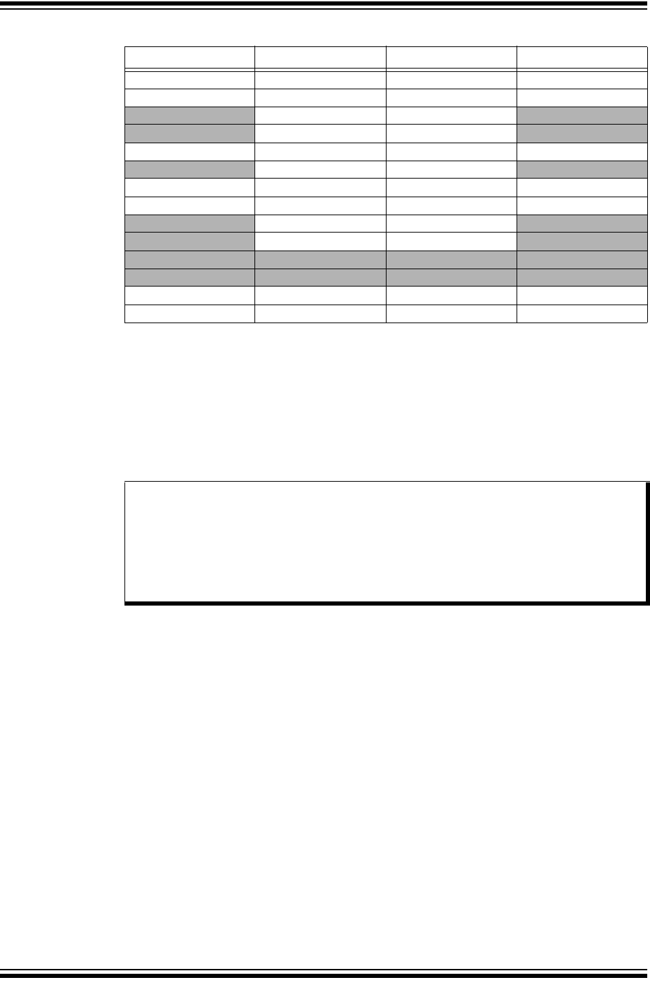
TABLE A-21: PIC16F917 PIN AND PORT COMPARISON
A.3 LED DISPLAY
Two green LEDs are connected to RC3 and RC4 of U1A through the J14 pins, 1, 2 and
7, 8 (outer ends), respectively.
One green LED is provided to determine whether there is power to the LCD 2
Demonstration Board (LED on) or not (LED off).
A.4 CHARGE PUMP AND VLCAP
For charge pump mode operation in PIC18F85J90 and PIC18F87J90 devices, it is
required that RC3 and RC4 of U1A connect to charge pump capacitor C7 through the
J14 pins, 3, 4 and 5, 6 (inner pins), respectively.
A.5 RESISTIVE LADDER VERSUS CHARGE PUMP
The switch, S6, allows the connection of either the resistor ladder or the capacitors to
the BIAS pins to generate the BIAS voltages for the LCD operation. For the Charge
Pump mode operation in PIC18F85J90 and PIC18F87J90 devices, it is required that
the S6 switch is flipped towards C and the VLCAP is connected through the inner
jumpers of J14. For the resistor ladder, S6 must be flipped towards R. The R45
potentiometer controls the contrast to the LCD in the Resistive Ladder mode.
A.5.1 Jumper JP21
When jumper JP21 is on, the LCDBIAS0 is physically tied to ground. The jumper needs
to be on for PIC18F85J90 and PIC18F87J90 devices when the bias voltages are
generated through the resistor ladder.
PIC16F917 Port PIC16F917 Pin ICE Pin ICE Port
RA0 AN0 AN0 RA0
RA1 AN1 AN1 RA1
RA6 T1OSCO T1OSCO RC0
RA7 T1OSCI T1OSCI RC1
RB0 RB0 RB0 RB0
RB5 COM1 COM1 RE4
RB6 RB6 RB6 RB6
RB7 RB7 RB7 RB7
RC0 VLCD1 BIAS1 RE0
RC1 VLCD2 BIAS2 RE1
RC3 SEG6 SEG11 RB4
RC4 SEG11 SEG14 RA4
RC6 TX/CK TX/CK RC6
RC7 RX/DT RX/DT RC7
Legend: Unshaded cells indicate a perfect match between the PIM and the glass.
Shaded cells indicate the pins that are remapped to the corresponding pin on the PIM.
Note 1: For the PIC18F85J90 and PIC18F87J90 PIM, the RG2 and RG3 pins are
connected to RC3 and RC4 of U1A, respectively.
2: For the PIC16F17 PIM, the RD1 and RD2 pins are connected to RC3 and
RC4 of U1A, respectively.
3: For the PIC18F8490 PIM, the RC3 and RD4 pins are connected to RC3
and RC4 of U1A, respectively