
User manual


Table Of Contents
- Chapter 1. Introduction
- Chapter 2. Getting Started
- Chapter 3. Using the Demo Software
- Appendix A. Board Technical Information
- Figure A-1: PICDEM™ LCD 2 Default Jumper Location
- A.1 Processors
- A.2 LCD Display
- Figure A-2: PICDEM™ LCD 2 Display
- Table A-2: LCD Glass Specifications
- Figure A-3: Display Definitions
- Figure A-4: Digit Description
- Table A-3: LCD SEGx and COMx
- A.2.1 Device-Specific LCD Segment Configuration
- Table A-4: PIC18F85J90 PIM and ICE Pin/Port Comparison
- Table A-5: PIC18F85J90 LCD connections Comparison
- Figure A-5: Segment Configuration for PIC18F85J90 Devices
- Table A-6: PIC18F85j90 pORT AND pIN cOMPARISON
- Table A-7: PIC18F87J90 PIM and ICE Pin/Port Comparison
- Table A-8: PIC18F87J90 LCD connections Comparison
- Figure A-6: Segment Configuration for PIC18F87J90 Devices
- Table A-9: PIC18F87j90 pORT AND pIN cOMPARISON
- Table A-10: PIC18F8490 Pim and ICE Port/Pin Comparison
- Table A-11: pic18f8490 LCD cONNECTIONS cOMPARISON
- Figure A-7: Segment Configuration for PIC18F8490 Devices
- Table A-12: pic18f8490 pIN AND pORT cOMPARISON
- Table A-13: PIC16F946 PIM and ICE PIn/Port Comparison
- Table A-14: PIC16F946 LCD Connections cOMPARISON
- Figure A-8: Segment Configuration for PIC16F946 Devices
- Table A-15: pic16f946 pORT AND PIN cOMPARISON
- Table A-16: PIC16F/LF1946/7 PIM and ICE PIn/Port Comparison
- Table A-17: PIC16F/LF1946/7 LCD Connections cOMPARISON
- Figure A-9: Segment Configuration for PIC16F/LF1946/7 Devices
- Table A-18: pic16f/LF1946/7 pORT AND PIN cOMPARISON
- Table A-19: PIC16F917 PIM and ICE Pin/Port Comparison
- Table A-20: pic16f917 LCD cONNECTIONS cOMPARISON
- Figure A-10: Segment Configuration for PIC16F914/917 Devices
- Table A-21: pic16f917 pIN AND pORT cOMPARISON
- A.3 LED Display
- A.4 Charge Pump and VLCAP
- A.5 Resistive Ladder Versus Charge Pump
- A.6 Oscillator Options
- A.7 RS-232 Serial Port
- A.8 Real-Time Clock
- A.9 Serial EEPROM
- A.10 Analog Input
- A.11 Temperature Sensor
- A.12 Switches
- A.13 ICD Connector
- A.14 Power Supply
- A.15 Board Layout and Schematics
- A.16 PIM Layout and Schematics
- Figure A-16: PIC18F65J90 and PIC18F85J90 PIM Layout
- Figure A-17: PIC16F914/917 PIM Layout
- Figure A-18: PIC16F946 PIM Layout
- Figure A-19: PIC16F/LF1946/7 PIM Layout
- Figure A-20: PIC18F6490/8490 PIM Layout
- Figure A-21: PIC18F87j90 PIM Layout
- Figure A-22: PICDEM™ LCD 2 PIC16F914/917 PIM Schematic
- Figure A-23: PICDEM LCD 2 PIC16F/LF1946/7 64-Pin PIM Schematic
- Figure A-24: PICDEM™ LCD 2 PIC16F946 PIM Schematic
- Figure A-25: PICDEM™ LCD 2 PIC18F6490 64-pin PIM Schematic
- Figure A-26: PICDEM™ LCD 2 PIC18F8490 80-pin PIM Schematic
- Figure A-27: PICDEM™ LCD 2 PIC18F6XJ90 64-pin PIM Schematic
- Figure A-28: PICDEM™ LCD 2 PIC18F87J90 80-pin PIM Schematic
- Figure A-29: PICDEM™ LCD 2 PIC18F85J90 80-pin PIM Schematic
- Worldwide Sales and Service
Board Technical Information
2010 Microchip Technology Inc. DS51662C-page 43
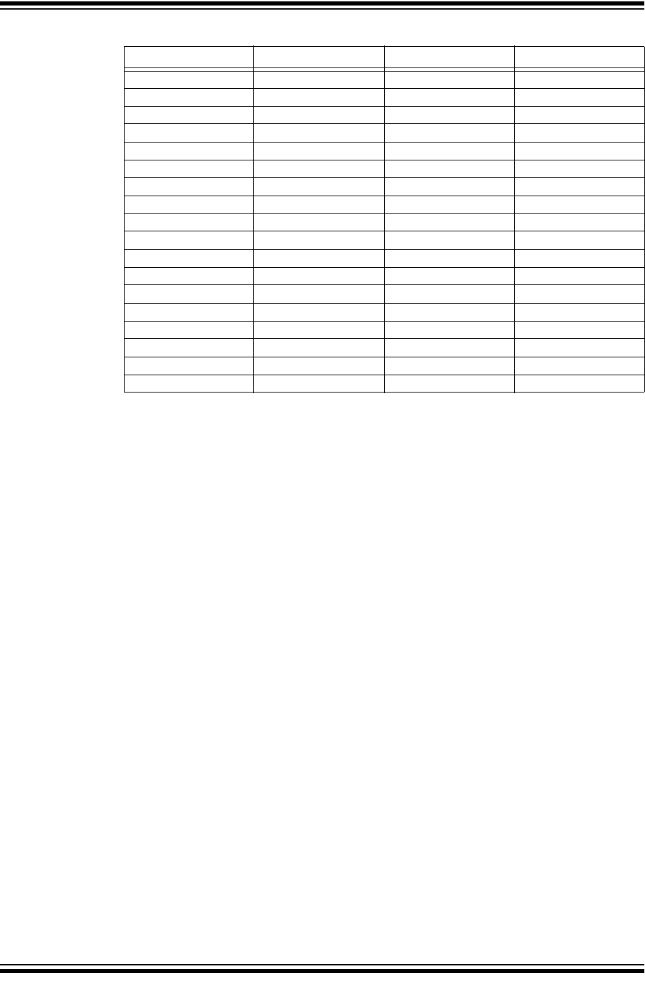
TABLE A-18: PIC16F/LF1946/7 PORT AND PIN COMPARISON
PIC16F/LF1946/7 Port PIC16F/LF1946/7 Pin ICE Pin ICE Port
RA0 AN0 AN0 RA0
RA1 AN1 AN1 RA1
RC0 T1OSCO T1OSCO RC0
RC1 T1OSCI T1OSCI RC1
RB0 RB0 RB0 RB0
RE3 COM0 COM0 RE3
RB5 COM1 COM1 RE4
RE5 COM2 COM2 RE5
RE6 COM3 COM3 RE6
RB6 RB6 RB6 RB6
RB7 RB7 RB7 RB7
RE0 VLCD1 BIAS1 RE0
RE1 VLCD2 BIAS2 RE1
RE2 VLCD3 BIAS3 RE2
RC3 RC3 RC3 RC3
RC4 RC4 RC4 RC4
RC6 TX/CK TX/CK RC6
RC7 RX/DT RX/DT RC7
Legend: Unshaded cells indicate a perfect match between the PIM and the glass.
Shaded cells indicate the pins that are remapped to the corresponding pin/port on the PIM.