
User manual


Table Of Contents
- Chapter 1. Introduction
- Chapter 2. Getting Started
- Chapter 3. Using the Demo Software
- Appendix A. Board Technical Information
- Figure A-1: PICDEM™ LCD 2 Default Jumper Location
- A.1 Processors
- A.2 LCD Display
- Figure A-2: PICDEM™ LCD 2 Display
- Table A-2: LCD Glass Specifications
- Figure A-3: Display Definitions
- Figure A-4: Digit Description
- Table A-3: LCD SEGx and COMx
- A.2.1 Device-Specific LCD Segment Configuration
- Table A-4: PIC18F85J90 PIM and ICE Pin/Port Comparison
- Table A-5: PIC18F85J90 LCD connections Comparison
- Figure A-5: Segment Configuration for PIC18F85J90 Devices
- Table A-6: PIC18F85j90 pORT AND pIN cOMPARISON
- Table A-7: PIC18F87J90 PIM and ICE Pin/Port Comparison
- Table A-8: PIC18F87J90 LCD connections Comparison
- Figure A-6: Segment Configuration for PIC18F87J90 Devices
- Table A-9: PIC18F87j90 pORT AND pIN cOMPARISON
- Table A-10: PIC18F8490 Pim and ICE Port/Pin Comparison
- Table A-11: pic18f8490 LCD cONNECTIONS cOMPARISON
- Figure A-7: Segment Configuration for PIC18F8490 Devices
- Table A-12: pic18f8490 pIN AND pORT cOMPARISON
- Table A-13: PIC16F946 PIM and ICE PIn/Port Comparison
- Table A-14: PIC16F946 LCD Connections cOMPARISON
- Figure A-8: Segment Configuration for PIC16F946 Devices
- Table A-15: pic16f946 pORT AND PIN cOMPARISON
- Table A-16: PIC16F/LF1946/7 PIM and ICE PIn/Port Comparison
- Table A-17: PIC16F/LF1946/7 LCD Connections cOMPARISON
- Figure A-9: Segment Configuration for PIC16F/LF1946/7 Devices
- Table A-18: pic16f/LF1946/7 pORT AND PIN cOMPARISON
- Table A-19: PIC16F917 PIM and ICE Pin/Port Comparison
- Table A-20: pic16f917 LCD cONNECTIONS cOMPARISON
- Figure A-10: Segment Configuration for PIC16F914/917 Devices
- Table A-21: pic16f917 pIN AND pORT cOMPARISON
- A.3 LED Display
- A.4 Charge Pump and VLCAP
- A.5 Resistive Ladder Versus Charge Pump
- A.6 Oscillator Options
- A.7 RS-232 Serial Port
- A.8 Real-Time Clock
- A.9 Serial EEPROM
- A.10 Analog Input
- A.11 Temperature Sensor
- A.12 Switches
- A.13 ICD Connector
- A.14 Power Supply
- A.15 Board Layout and Schematics
- A.16 PIM Layout and Schematics
- Figure A-16: PIC18F65J90 and PIC18F85J90 PIM Layout
- Figure A-17: PIC16F914/917 PIM Layout
- Figure A-18: PIC16F946 PIM Layout
- Figure A-19: PIC16F/LF1946/7 PIM Layout
- Figure A-20: PIC18F6490/8490 PIM Layout
- Figure A-21: PIC18F87j90 PIM Layout
- Figure A-22: PICDEM™ LCD 2 PIC16F914/917 PIM Schematic
- Figure A-23: PICDEM LCD 2 PIC16F/LF1946/7 64-Pin PIM Schematic
- Figure A-24: PICDEM™ LCD 2 PIC16F946 PIM Schematic
- Figure A-25: PICDEM™ LCD 2 PIC18F6490 64-pin PIM Schematic
- Figure A-26: PICDEM™ LCD 2 PIC18F8490 80-pin PIM Schematic
- Figure A-27: PICDEM™ LCD 2 PIC18F6XJ90 64-pin PIM Schematic
- Figure A-28: PICDEM™ LCD 2 PIC18F87J90 80-pin PIM Schematic
- Figure A-29: PICDEM™ LCD 2 PIC18F85J90 80-pin PIM Schematic
- Worldwide Sales and Service
PICDEM™ LCD 2 Demonstration Kit User’s Guide
DS51662C-page 26 2010 Microchip Technology Inc.
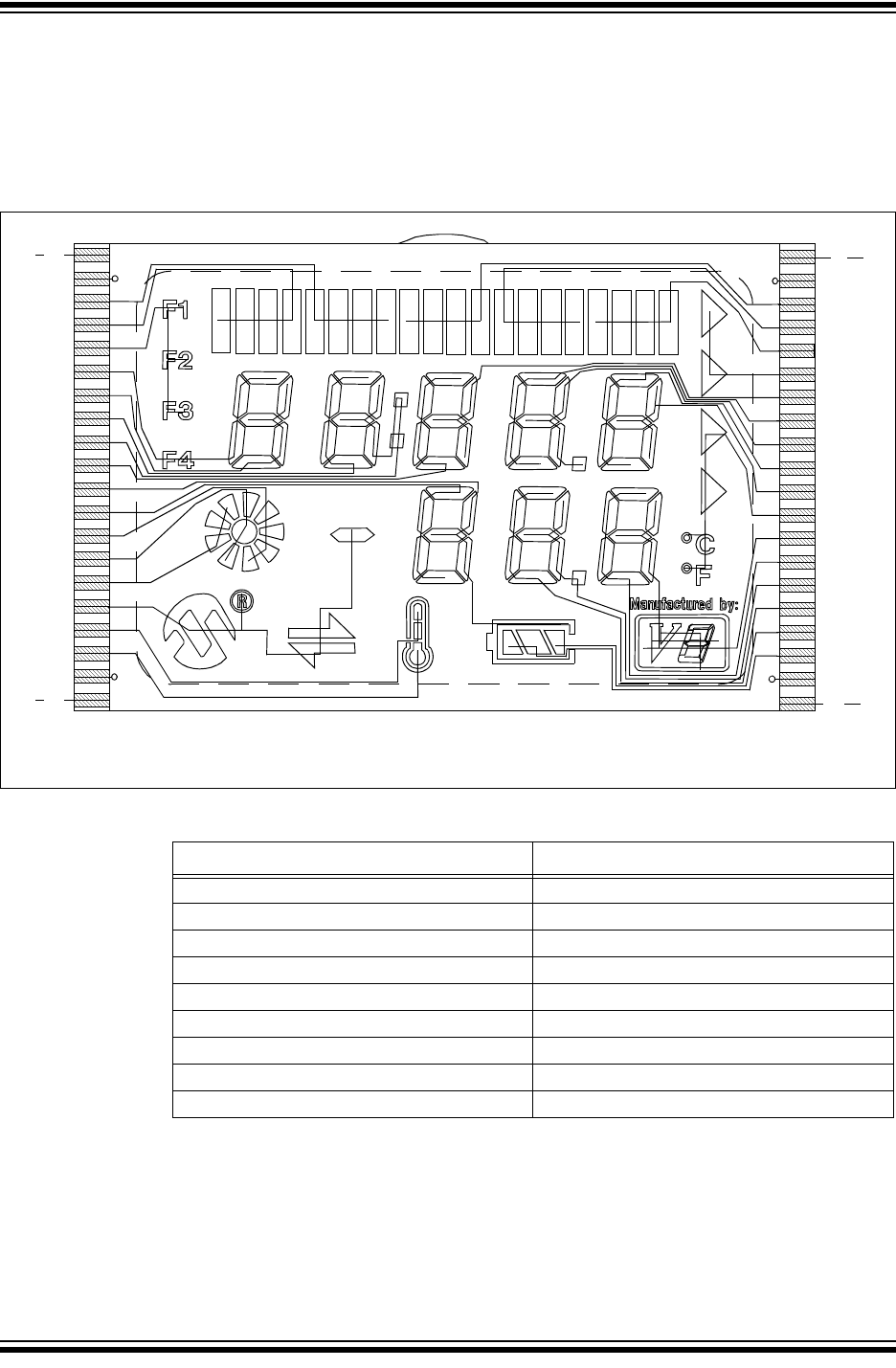
A.2 LCD DISPLAY
A custom-made segmented LCD glass, manufactured by the Varitronix Corporation, is
provided as shown in Figure A-2. This LCD has 4 commons and 32 segments.
Table A-2 provides a few of the specifics for the display. Refer to the Varitronix
specification sheet (VL_5573_V00) for additional details.
FIGURE A-2: PICDEM™ LCD 2 DISPLAY
Since the glass used on the PICDEM LCD 2 operates at 3V, there is a voltage protec-
tion circuit on the LCDBIAS3 pin, which is enabled in the default configuration. When
enabled, even if the V
DD is greater than 3V, it regulates the LCDBIAS3 voltage such
that it always maintains the value to 3V. This is not necessary for operation of the LCD
module, but it is a protection circuit to prevent accidentally applying voltages higher
than 3V to the LCD glass present on the board.
40
N.C.
21
N.C.
20
N.C.
1
N.C.
COM1
SEG15
SEG14
SEG13
SEG12
SEG11
SEG10
SEG9
SEG8
SEG7
SEG6
SEG5
SEG4
SEG3
SEG2
SEG1
SEG0
COM0
COM2
SEG16
SEG17
SEG18
SEG19
SEG20
SEG21
SEG22
SEG23
SEG24
SEG25
SEG26
SEG27
SEG28
SEG29
SEG30
SEG31
COM3
Legend: N.C. = No connection
© VL Electronics
TABLE A-2: LCD GLASS SPECIFICATIONS
Type Specification
P.I.D. VL_5573_V00
Mode/Color/Type Positive / -- / TN
Viewing Direction 6:00 O’Clock
Driving Scheme 1/4 Duty, 1/3 Bias
Drive Voltage (VLCD) ~3.0 Volt (p-p), +20°C
Operating Temperature 0°C - +50°C
Storage Temperature -10°C - +60°C
Polarizer – Front STD.Transmissive
Polarizer – Back STD.Reflective