
User manual

Atmel AVR1925: XMEGA-C3 Xplained Hardware User’s Guide [APPLICATION NOTE]
42053A−AVR−02/2013
7
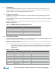
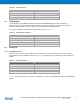
The header J2 is connected to analog ports of the XMEGA as shown in Table 3-3.
Table 3-3. Expansion header J2.
Pin on J2 Name on J2 XMEGA pin Shared with onboard functionality
1 ADC0 PB0 -
2 ADC1 PB1 -
3 ADC2 PB2 -
4 ADC3 PB3 -
5 ADC4 PB4 -
6 ADC5 PB5 -
7 ADC6 PB6 -
8 ADC7 PB7 -
9 GND - -
10 VCC_P3V3 - -
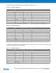
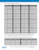
The header J3 is connected to digital ports of XMEGA. Table 3-4 shows the mapping of the XMEGA I/O to J3.
Table 3-4. Expansion header J3.
Pin on J3 Name on J3 XMEGA pin Shared with onboard functionality
1 PA0 PA0 Light sensor
(1)
2 PA1 PA1 Temperature sensor
(1)
3 PA2 PA2 Filter output
(1)
4 PA3 PA3 Display reset
5 PA4 PA4
6 PA5 PA5
7 PA6 PA6
8 PA7 PA7
9 GND - -
10 VCC_P5V0 - -
Note: 1. Can be disconnected from onboard functionality by cut-straps.
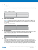
The header J4 offers digital communication interfaces such as UART and TWI but care must be taken because some
pins are also connected to on-board peripherals.
Table 3-5. Expansion header J4.
Pin on J4 Name on J4 XMEGA pin Shared with onboard functionality
1 SDA PE0 -
2 SCL PE1 -
3 RXD PE2 -
4 TXD PE3 -
5 SS PD0 Display data and command select
(1)
6 MOSI PD3 Display and microSD card MOSI
7 MISO PD2 microSD card MISO
8 SCK PD1 Display and microSD card clock input
9 GND - -
10 VCC_P3V3 - -
Note: 1. Can be disconnected from onboard functionality by cut-strap (J204).