
Datasheet


511
32133D–11/2011
UC3D
25.7 User Interface
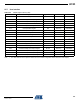
Note: 1. The reset values are device specific. Please refer to the Module Configuration section at the end of this chapter.
Table 25-3. PWMA Register Memory Map
Offset Register Register Name Access Reset
0x00 Control Register CR Read/Write 0x00000000
0x04 Interlinked Single Value Duty Register ISDUTY Write-only 0x00000000
0x08 Interlinked Multiple Value Duty Register IMDUTY Write-only 0x00000000
0x0C Interlinked Multiple Value Channel Select IMCHSEL Write-only 0x00000000
0x10 Interrupt Enable Register IER Write-only 0x00000000
0x14 Interrupt Disable Register IDR Write-only 0x00000000
0x18 Interrupt Mask Register IMR Read-only 0x00000000
0x1C Status Register SR Read-only 0x00000000
0x20 Status Clear Register SCR Write-only 0x00000000
0x24 Parameter Register PARAMETER Read-only -
(1)
0x28 Version Register VERSION Read-only -
(1)
0x2C Top Value Register TVR Read/Write 0x00000000
0x30+m*0x10 Interlinked Single Value Channel Set m ISCHSETm Write-only 0x00000000
0x3C+k*0x10 CWG Register CWGk Read/Write 0x00000000
0x80 Interlinked Multiple Value Duty0 Register DUTY0 Write-only 0x00000000
0x84 Interlinked Multiple Value Duty1 Register DUTY1 Write-only 0x00000000
0x88 Interlinked Multiple Value Duty2 Register DUTY2 Write-only 0x00000000
0x8C Interlinked Multiple Value Duty3 Register DUTY3 Write-only 0x00000000