
User manual


If other voltages are required, the kit must be disconnected from the USB to avoid damage or contention
to the USB power. The mEDBG must also be disconnected from the target section of the board. The
board can be power by applying a voltage to one of the power connections on the board according to the
table below. To avoid any power leakage through the mEDBG, this should also be disconnected by
removing the resistors shown in Figure 3-3 Kit Modifications on page 8. For placement of power
connections, see Xplained Nano Standard Pin-Out on page 6.
Table 3-2. Power Connections
Power
Connection
Description
VUSB USB Voltage output when USB is connected (behind a PTC fuse). Can be used as
power input when USB is not used.
VREG Regulated voltage from VUSB. If the kit does not have a regulator, this is directly
connected to VUSB.
VCC Target voltage supply. By default connected to VREG through a 0Ω resistor. Apply
external voltage here if the resistor is removed.
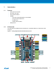
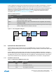
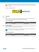
Figure 3-1. Power Supply Block Diagram
USB Target MCUPTC
Power source
Power connection
Power consumer
0-ohm Resistor
VUSB /
VREG
VCC
mEDBG
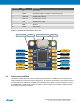
3.3. Xplained Nano Standard Pin-Out
Xplained Nano kits have a standard pin-out in the mEDBG section as shown in the tables and figure
below. The program/debug pins will change depending on the target interface, but will remain at the same
locations.
Xplained Nano kits have a target section where all I/O pins will be available and fanned out. Except for
the VCC and GND pins with fixed positions, there are no defined pin functions in this area. The first pin in
the target area is the VCC pin, located right next to the VREG pin of the standard section. The last pin is
GND, and it's located next to the CDC RX pin in the stadard section. For reference, see figure below.
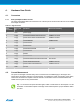
3.3.1. Standard Pin-Out for TPI
Table 3-3. Xplained Nano mEDBG Standard Pin-Out
Pin number Name Description
1 RST Reset line
2 TPID TPI Program data line
3 TPIC TPI Program clock output
Atmel ATtiny104 Xplained Nano [USER GUIDE]
Atmel-42671A-ATtiny104-Xplained-Nano_User Guide-02/2016
6