
User manual


8
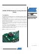
AVR600
8170A-AVR-08/08
STK600 Signal name MCU Comment
TGT_SCK, TGT_MISO,
TGT_MOSI ISP pins ISP programming interface
TGT_TDI, TGT_TDO,
TGT_TMS, TGT_TCK JTAG pins JTAG programming interface
VBUST VBUS VBUS (sense) for USB
UID UID ID pin for USB OTG
UVCON UVCON
USB VBUS generation control for
USB OTG. A low level on this
signal enables VBUS generation.
DP, DN DP, DN USB differential pair
TGT_PDATAx (HV) data pins
Data pins for high voltage
(PP/HVSP) programming.
TGT_CTRL0 (HV) Byte Select 2
TGT_CTRL1 (HV) Ready
TGT_CTRL2 (HV) Output Enable
TGT_CTRL3 (HV) Write Enable
TGT_CTRL4 (HV) Byte Select 1
TGT_CTRL5 (HV) XTAL0
TGT_CTRL6 (HV) XTAL1
TGT_CTRL7 (HV) PAGEL
Control signals for High voltage
Parallell Programming / Serial
Programming. Please refer to
AVR datasheet for further
information.
On AVRs with common BS1 /
PAGEL, BS1 is used.
BOARD_IDn none
ID system for router / socket /
expansion cards, see section 5 -
ID System
Notes: 1. Not all AVR will have every pin (ex. two aref pins, tosc or usb)
2. A MCU pin will fan-out to both Pnx pin and to the programming interface(s)
located at that pin.
3 Socket cards
Socket cards route each pin from the IC socket to separate pins on the spring loaded
connectors on the bottom side, facing the routing card.
3.1 Power design issues
Since all routing is handled by the routing card, even power lines and power
decoupling is ignored at the socket card. This produces less than ideal power design
which may lead to unwanted noise, ground bounce and other effects. It should
therefore be expected that heavily loaded designs can not run at full speed on
STK600. Likewise, such power design is not recommended for custom designs.
3.2 Connector MPN
Table 3-1. Socket card connector
Manufacturer and MPN Quantity Comment
SAMTEC, FSI-140-03-G-D-AD 2 Spring loaded 80-pin connector