Atmel SAM4S-WPIR-RD ....................................................................................................................
Section 1 1.1 Scope ................................................................................................................................. 1-1 1.2 References and Applicable Documents ............................................................................. 1-2 Section 2 2.1 Deliverables ....................................................................................................................... 2-3 2.2 Board Specifications .....................................................
Section 1 Introduction 1.1 Scope The SAM4S-WPIR-RD Reference Design Kit is based on SAM4S16C device. It introduces the application of Passive InfraRed Motion Detector Camera. This User Guide gives design details on the Reference Design Kit and is made up of 4 sections: Section 1 includes a photo of the board, references and applicable documents. Section 2 describes the contents and the main features of the Reference Design Kit.
1.2 References and Applicable Documents Table 1-1. References and Applicable Documents Title SAM4S datasheet Comment http://www.atmel.com/products/microcontrollers/arm/sam4s.
Section 2 Kit Contents 2.1 Deliverables The Atmel® SAM4S-WPIR-RD Reference Design Kit includes: Board – One SAM4S-WPIR-RD board Power supply – USB supply Cables – One USB cable, type A to type Micro-B Unpack and inspect the kit carefully. Contact your local Atmel distributor, should there be issues concerning the contents of the kit. 2.2 Board Specifications Table 2-1.
2.3 Electrostatic Warning The SAM4S-WPIR-RD board is shipped in a protective anti-static package. The board system must not be subjected to high electrostatic potentials. A grounding strap or similar ESD protective device should be worn when handling the board in hostile ESD environments (offices with synthetic carpet, for example). Avoid touching the component pins or any other metallic element on the board.
Section 3 Power Up 3.1 Power Up the Board Unpack the board taking care to avoid electrostatic discharge. Connect the board to PC with the USB cable, or insert 3 x AAA Alkaline cells on U4 Battery Holder, and then the board should be powered on. Note: 3.2 Jumpers JP1, JP4, JP7, JP8, JP9, JP10 must be closed and JP2, JP3 must be open for start-up. Sample Code and Technical Support Users can download sample code and get technical support from the Atmel web site: http://www.atmel.
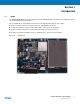
Section 4 Hardware 4.1 Introduction The SAM4S-WPIR-RD block diagram includes battery holder, LDO, image sensor, 1M byte SRAM, PIR sensor, JTAG connector, LCD, ZigBee connector, as shown in Figure 4-1. Figure 4-1. SAM4S-WPIR-RD Block Diagram 4.2 Function Blocks 4.2.1 Processor The board is equipped with a SAM4S16 device in a LQFP100 package.
4.2.2 Clock Circuitry The board includes 2 clock sources: One 12 MHz Crystal for Internal Clock (Y2) One 32.768 kHz Crystal for RTC Clock (Y1) 4.2.3 Reset Circuitry The reset sources for the board are: Power on reset JTAG reset from an in-circuit emulator (JTAG interface is equipped on the board) 4.2.4 Push Button Switches 4.2.5 User interface (BP1) Power Supplies The Board is driven by 5V input power rail from USB cable or 3 x AAA battery.
Power Supply Figure 4-2. J1 USB Micro B 4 3 2 FGND 1 RV1 5V D- D+ ID 7 6 G VIN_SYSTEM 1 C59 1uF 5 8 9 R43 100K V5.5MLA0603 R2 68K C3 10pF RV2 V5.
4.2.7 JTAG/ICE Software debug is accessed by a standard 20-pin JTAG connection. This allows connection to a standard USB-toJTAG in-circuit emulator such as SAM-ICE™. Figure 4-4. JTAG Interface +3V_MCU R6 J2 2 4 6 8 10 12 14 16 18 20 1 100K 3 5 7 9 11 13 15 17 19 R7 R8 R9 R10 100K 100K 100K 100K TDI TMS TCK TDO NRST HTST-110-01-SM-DV DGND 4.2.
PIR Sensor Figure 4-6.
4.2.10 ZigBee The board has a 10-pin male connector for the Atmel RZ600 ZigBee module. ZigBee Interface Figure 4-7. ZB_RSTN ZB_IRQ SPIO_NPCS1# MISO PA5 PB2 PB14 PA12 1 3 5 7 9 J5 2X10PTS COUDE 2 4 6 8 10 PB3 PA6 PA13 PA14 C61 18pF C62 2.2nF MISC SLP_TR MOSI SPCK +3V_PERIPH C63 2.2uF DGND 4.2.11 LED Indicators The board has one LED indicator for purposes shown below: Table 4-2. LED Indicators 4.2.
Figure 4-8. LCD Block 1 2 3 4 5 6 7 8 9 10 11 12 13 14 15 16 17 18 19 20 21 22 23 24 25 26 27 28 29 30 31 32 33 34 35 36 37 38 39 PC7 PC6 PC5 PC4 PC3 PC2 PC1 PC0 +3V_LCD + C52 10uF C53 100nF C54 100nF R44 47K +3V_LCD DGND R54 10K PC11 PC8 PC19 NCS2PA22 NRST LED_A R57 4.7K R56 0R LED_K1 LED_K2 LED_K3 LED_K4 DGND DGND 4.2.13 J4 FH26-39S-0.
Figure 4-9. Backlight Control MN10 +3V_LCD 10 C64 1uF R58 47K R59 0R PC13 +3V_LCD 9 11 5 B2 BN03K314S300R C67 4.7uF 4 C1+ C1EN/SET 7 C2+ 6 C2OUTCP IN GND AAT3155ITP D1 D2 D3 D4 C65 1uF 8 LED_A 3 2 1 12 LED_K1 LED_K2 LED_K3 LED_K4 C66 1uF DGND DGND 4.3 Connectors 4.3.1 JTAG/ICE Connector Figure 4-10. JTAG J2 Table 4-3. JTAG/ICE Connector J2 Signal Descriptions Pin Mnemonic Description 1 VTref. 3.3V power This is the target reference voltage.
Pin Mnemonic Description 10 GND Common ground 11 RTCK - Input Return test clock signal from the target. Some targets must synchronize the JTAG inputs to internal clocks. To assist in meeting this requirement, a returned and retimed TCK can be used to dynamically control the TCK rate. SAM-ICE supports adaptive clocking which waits for TCK changes to be echoed correctly before making further changes. Connect to RTCK if available, otherwise to GND.
4.3.3 ZigBee Socket J5 ZigBee Socket J5 Figure 4-12. Table 4-5. ZigBee Socket J5 Signal Descriptions 4.3.4 Function Signal Name Signal Name Function Reset 2 Misc. Interrupt Request 3 4 SLP_TR SLP_TR /SEL 5 6 MOSI SPI MOSI SPI MISO MISO 7 8 SCLK SPI CLK Power Supply GND 9 10 VCC VCC Port Pin Pin /RST 1 Interrupt Request IRQ1 SPI chip select GND Port VCC LCD/TSC Socket J4 LCD/TSC Socket J4 Figure 4-13. Table 4-6.
Mnemonic Pin Num Pin Num Mnemonic RD PC11 21 22 PC8 WR RS PC19 23 24 PA22 CS RESET NRST 25 26 PULL UP IM0 IM1 PULL DOWN 27 28 GND GND LED-A LED-A 29 30 LED-K1 LED-K1 LED-K2 LED-K2 31 32 LED-K3 LED-K3 LED-K4 LED-K4 33 34 NC Y UP Y DOWN NC 35 36 NC X RIGHT X LEFT NC 37 38 NC NC GND GND 39 SAM4S-WPIR-RD [USER GUIDE] 42060A–ATARM–12/2012 16
Schematics 4.
VIN_SYSTEM 5 TP1 TP2 C1 15pF C2 15pF 15pF DGND C4 15pF 0R R11 XIN32 XIN TEST 4 +1V2 PB12_PWML1_ERASE PB0_PWMH0_AD12B4 PB1_PWMH1_AD12B5 NRST PB4_TWD1_PWMH2_TDI PB6_TMS_SWDIO PB7_TCK_SWCLK PB5_TWCK1_PWML0_TDO JTAGSEL PB11_DDP PB10_DDM PB3_UTXD1_PCK2_AD12B7 PB2_URXD1_NPCS2_AD12B6 PB8_XOUT PB9_XIN MN1 AT91SAM4S-LQFP100 97 96 88 XOUT 7 PB10 89 9 PB11 77 51 79 83 76 60 3 5 ERASE 87 61 +3V_MCU + +3V_MCU VDDCORE JP7 +3V_PERIPH JP4 JP9 +1V2 DGND Y2 12M XOUT32 Y1 32.
D C B A PC15 PB13 FSIN HREF VSYNC PA23 PA21 PA16 PA15 PB13 {2} {2} {2} {2} PA4 PA3 {2} {2} {2} {2} XVCLK1 PCLK {2} {2} {2} {2} {2} {2} {2} {2} +3V_LCD R54 {2} 10K {2} {2} {2} {2} R57 4.7K DGND 5 R29 4.
Section 5 Revision History 5.
Atmel Corporation 1600 Technology Drive Atmel Asia Limited Unit 01-5 & 16, 19F Atmel Munich GmbH Business Campus Atmel Japan G.K. 16F Shin-Osaki Kangyo Bldg San Jose, CA 95110 BEA Tower, Millennium City 5 Parkring 4 1-6-4 Osaki, Shinagawa-ku USA 418 Kwun Tong Roa D-85748 Garching b. Munich Tokyo 141-0032 Tel: (+1) (408) 441-0311 Kwun Tong, Kowloon GERMANY JAPAN Fax: (+1) (408) 487-2600 HONG KONG Tel: (+49) 89-31970-0 Tel: (+81) (3) 6417-0300 www.atmel.