
User manual


Evaluation Kit Hardware
SAM4S-EK2 User Guide 4-8
11176A–ATARM–24-Sep-12
4.3.8.3 Touch Screen Interface
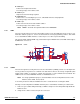
The LCD module integrates a 4-wire touch panel controlled by MN7 (ADS7843) which is a slave device
on the SAM4SD32 SPI bus. The controller sends back the information about the X and Y positions, as
well as a measurement for the pressure applied to the touch panel. The touch panel can be used with
either a stylus or a finger.
The ADS7843 touch panel controller connects to the SPI0 interface via the NPCS0 control signal. Two
interrupt signals are connected and provide events information back to the microcontroller: PenIrq and
Busy.
Note: PenIrq (PA16) is shared with ZigBEE signal IRQ0.
Busy (PA17) is shared with ZigBEE signal IRQ1.
Therefore, if using a ZigBEE interface in concurrence with the TouchScreen controller, take
care not to have both drivers enabled at the same time on either PA16 or PA17.
For that purpose, 0 Ohm resistors have been implemented on these PIO lines in order to disconnect
either end driver from the other:
On the touch panel controller side, R67 and R69.
On ZigBEE side, R117 and R120.
For further information, refer to the “Schematics” section.
Touch ADC auxiliary inputs IN3/IN4 of the ADS7843 are connected to test points (TP8, TP9) for optional
function extension.
Figure 4-10. Touch Panel Control
4.3.9 JTAG/ICE
A standard 20-pin JTAG/ICE connector is implemented on the SAM4S-EK2 for the connection of a com-
patible ARM JTAG emulator interface, such as the SAM-ICE from Segger.
Notes: 1. The NRST signal is connected to BP1 system button and is also used to reset the LCD
module. The 0 ohm resistor R44 may be removed in order to isolate the JTAG port from
this system reset signal.
2. The TDO pin is in input mode with the pull-up resistor disabled when the Cortex M4 is
not in debug mode. To avoid current consumption on VDDIO and/or VDDCORE due to
floating input, the internal pull-up resistor corresponding to this PIO line must be
enabled.
AGND_TP
JP 32
Heade r2
LCD TOUCH SCREEN
R7 4
0R
C5 9
100nF
C5 8
100nF
R7 1
1R
C6 0
100nF
TP 8
PA14
PA13
PA12
C6 1
4.7uF
PA11
PA17
TP 9
DG ND
R6 5
100K
+3V3
+3V3
AGND_TP
+3V3
R6 2
100K
R7 3
100K
R7 2
100K
L2
10uH-100mA
MN7
ADS7 843E
XP
2
YP
3
XM
4
YM
5
DCLK
16
DIN
14
DO UT
12
CS
15
BUSY
13
PE NIRQ
11
VREF
9
VCC1
1
VCC2
10
GND
6
IN3
7
IN4
8
X_RIGHT
Y_DOWN
X_LEFT
Y_UP
R6 7 0R
R7 0 0R
R6 9 0R
PA16