
User manual


Evaluation Kit Hardware
SAM4S-EK2 User Guide 4-7
11176A–ATARM–24-Sep-12
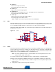
4.3.8.1 LCD Module
The LCD module gets reset from the NRST signal. As explained, this NRST is shared with the JTAG port
and the push-button BP1. The LCD chip select signal is connected to NCS1; the jumper JP13 can dis-
connect it so that this PIO line is available for other custom usage.
The SAM4SD32 communicates with the LCD through PIOC where an 8-bit parallel “8080-like” protocol
data bus has to be implemented in software.
Figure 4-8. LCD Block
4.3.8.2 Backlight Control
The LCD backlight is made of four integrated white chip-LEDs arranged in parallel. These are driven by
an AAT3155 charge pump, MN8. The AAT3155 is controlled by the SAM4SD32 through a single PIO
line PC13 interface; the 0 Ohm resistor R68 is mounted in series on this line, which permits to use it for
other custom purposes. In that case, the pull-up resistor R64 maintains the charge pump permanently
enabled by default.
On the anode drive line, a 0 Ohm resistor R59 is implemented in series for an optional current limitation.
Figure 4-9. Backlight Control
LCD_DB3
R5 9 0R
Six slots on PCB for LCD shield
PC11
R6 3 4.7 K
DNP
DG ND
LED_A
PC26
LCD_DB2
NRST
PC8
LCD_DB0
PC27
LCD
C4 5
100nF
LCD_DB4
DG ND
J8
FH26-39S-0.3SHW
VDD
1
DB 17
2
DB 16
3
DB 15
4
DB 14
5
DB 13
6
DB 12
7
DB 11
8
DB 10
9
DB 9
10
DB 8
11
DB 7
12
DB 6
13
DB 5
14
DB 4
15
DB 3
16
DB 2
17
DB 1
18
DB 0
19
VDD
20
RD
21
WR
22
RS
23
CS
24
RE SE T
25
IM0
26
IM1
27
GND
28
LED-A
29
LEDK1
30
LEDK2
31
LEDK3
32
LEDK4
33
Y+
34
Y-
35
X+
36
X-
37
NC
38
GND
39
PC28
DG ND
R4 9
47K
X_RIGHT
Y_DOWN
Y_UP
X_LEFT
D1
PACDN044Y5 R
TVS, SOT23-5
DNP
1
2
345
NOT POPULATED
The part i s pl aced as
close as possible to J8
DG ND
PC29
DG ND
DG ND
DG ND
JP13 Heade r2
LCD_DB9
LCD_DB13
LCD_DB12
LCD_DB11
LCD_DB10
LCD_DB16
LCD_DB15
LCD_DB14
PC30
LCD_DB17
R5 8
4.7K
LCD_DB5
PC2
PC1
PC0
PC3
X_LEFT
LCD_DB9
R5 6
10K
PC6
PC5
PC4
PC7
PC23
X_RIGHT
+3V3
DG ND
DG ND
LCD_DB7
Y_DOWN
LCD_DB8
Y_UP
RA 2
4.7Kx4
DNP
1
2
3
4 5
6
7
8
PC22
PC31
PC13
LCD_DB6
LCD_DB6
LCD_DB7
DG ND
PC15
PC [0..31]
LED_K4
LCD_DB8
LCD_DB4
LCD_DB5
LED_K3
LED_K2
PC24
PINs
on
BO T
PIN 39
PIN 1
Z7
FTM28 0C 34D
LCD_DB2
LCD_DB3
LCD_DB1
LED_K1
NRST
RA 3
4.7Kx4
DNP
1
2
3
4 5
6
7
8
PC19
LCD_DB0
LCD_DB1
C4 4
100nF
R6 1 4.7 K
DNP
DG ND
+3V3
+
C4 3
10uF
PC25
MN8
AAT3155ITP-T1
C1 +
10
C1 -
9
EN/SET
11
C2 +
7
C2 -
6
OUTCP
8
IN
5
GND
4
D1
3
D2
2
D3
1
D4
12
C5 5
1uF
C5 4
1uF
C5 7
4.7uF
C5 6
1uF
R6 8
0R
R6 4
47K
LED_A
LED_K1
+3V3
LED_K4
LED_K3
LED_K2
+3V3
PC13
DG ND
DG ND
TP 7
FB 1
BN03K 314S300R
LCD BACKLI GHT