
Datasheet


Table Of Contents
- Features
- Pin Configurations
- Overview
- Resources
- Data Retention
- About Code Examples
- Atmel AVR CPU Core
- AVR ATmega8 Memories
- System Clock and Clock Options
- Power Management and Sleep Modes
- System Control and Reset
- Interrupts
- I/O Ports
- Introduction
- Ports as General Digital I/O
- Alternate Port Functions
- Register Description for I/O Ports
- The Port B Data Register – PORTB
- The Port B Data Direction Register – DDRB
- The Port B Input Pins Address – PINB
- The Port C Data Register – PORTC
- The Port C Data Direction Register – DDRC
- The Port C Input Pins Address – PINC
- The Port D Data Register – PORTD
- The Port D Data Direction Register – DDRD
- The Port D Input Pins Address – PIND
- External Interrupts
- 8-bit Timer/Counter0
- Timer/Counter0 and Timer/Counter1 Prescalers
- 16-bit Timer/Counter1
- Overview
- Accessing 16-bit Registers
- Timer/Counter Clock Sources
- Counter Unit
- Input Capture Unit
- Output Compare Units
- Compare Match Output Unit
- Modes of Operation
- Timer/Counter Timing Diagrams
- 16-bit Timer/Counter Register Description
- Timer/Counter 1 Control Register A – TCCR1A
- Timer/Counter 1 Control Register B – TCCR1B
- Timer/Counter 1 – TCNT1H and TCNT1L
- Output Compare Register 1 A – OCR1AH and OCR1AL
- Output Compare Register 1 B – OCR1BH and OCR1BL
- Input Capture Register 1 – ICR1H and ICR1L
- Timer/Counter Interrupt Mask Register – TIMSK(1)
- Timer/Counter Interrupt Flag Register – TIFR(1)
- 8-bit Timer/Counter2 with PWM and Asynchronous Operation
- Serial Peripheral Interface – SPI
- USART
- Two-wire Serial Interface
- Analog Comparator
- Analog-to- Digital Converter
- Boot Loader Support – Read- While-Write Self- Programming
- Boot Loader Features
- Application and Boot Loader Flash Sections
- Read-While-Write and No Read- While-Write Flash Sections
- Boot Loader Lock Bits
- Entering the Boot Loader Program
- Addressing the Flash During Self- Programming
- Self-Programming the Flash
- Performing Page Erase by SPM
- Filling the Temporary Buffer (Page Loading)
- Performing a Page Write
- Using the SPM Interrupt
- Consideration While Updating BLS
- Prevent Reading the RWW Section During Self-Programming
- Setting the Boot Loader Lock Bits by SPM
- EEPROM Write Prevents Writing to SPMCR
- Reading the Fuse and Lock Bits from Software
- Preventing Flash Corruption
- Programming Time for Flash when using SPM
- Simple Assembly Code Example for a Boot Loader
- ATmega8 Boot Loader Parameters
- Memory Programming
- Program And Data Memory Lock Bits
- Fuse Bits
- Signature Bytes
- Calibration Byte
- Page Size
- Parallel Programming Parameters, Pin Mapping, and Commands
- Parallel Programming
- Enter Programming Mode
- Considerations for Efficient Programming
- Chip Erase
- Programming the Flash
- Programming the EEPROM
- Reading the Flash
- Reading the EEPROM
- Programming the Fuse Low Bits
- Programming the Fuse High Bits
- Programming the Lock Bits
- Reading the Fuse and Lock Bits
- Reading the Signature Bytes
- Reading the Calibration Byte
- Parallel Programming Characteristics
- Serial Downloading
- Serial Programming Pin Mapping
- Electrical Characteristics – TA = -40°C to 85°C
- Electrical Characteristics – TA = -40°C to 105°C
- ATmega8 Typical Characteristics – TA = -40°C to 85°C
- Active Supply Current
- Idle Supply Current
- Power-down Supply Current
- Power-save Supply Current
- Standby Supply Current
- Pin Pull-up
- Pin Driver Strength
- Pin Thresholds and Hysteresis
- Bod Thresholds and Analog Comparator Offset
- Internal Oscillator Speed
- Current Consumption of Peripheral Units
- Current Consumption in Reset and Reset Pulsewidth
- ATmega8 Typical Characteristics – TA = -40°C to 105°C
- Register Summary
- Instruction Set Summary
- Ordering Information
- Packaging Information
- Errata
- Datasheet Revision History
- Changes from Rev. 2486Z- 02/11 to Rev. 2486AA- 02/2013
- Changes from Rev. 2486Y- 10/10 to Rev. 2486Z- 02/11
- Changes from Rev. 2486X- 06/10 to Rev. 2486Y- 10/10
- Changes from Rev. 2486W- 02/10 to Rev. 2486X- 06/10
- Changes from Rev. 2486V- 05/09 to Rev. 2486W- 02/10
- Changes from Rev. 2486U- 08/08 to Rev. 2486V- 05/09
- Changes from Rev. 2486T- 05/08 to Rev. 2486U- 08/08
- Changes from Rev. 2486S- 08/07 to Rev. 2486T- 05/08
- Changes from Rev. 2486R- 07/07 to Rev. 2486S- 08/07
- Changes from Rev. 2486Q- 10/06 to Rev. 2486R- 07/07
- Changes from Rev. 2486P- 02/06 to Rev. 2486Q- 10/06
- Changes from Rev. 2486O-10/04 to Rev. 2486P- 02/06
- Changes from Rev. 2486N-09/04 to Rev. 2486O-10/04
- Changes from Rev. 2486M-12/03 to Rev. 2486N-09/04
- Changes from Rev. 2486L-10/03 to Rev. 2486M-12/03
- Changes from Rev. 2486K-08/03 to Rev. 2486L-10/03
- Changes from Rev. 2486J-02/03 to Rev. 2486K-08/03
- Changes from Rev. 2486I-12/02 to Rev. 2486J-02/03
- Changes from Rev. 2486H-09/02 to Rev. 2486I-12/02
- Changes from Rev. 2486G-09/02 to Rev. 2486H-09/02
- Changes from Rev. 2486F-07/02 to Rev. 2486G-09/02
- Changes from Rev. 2486E-06/02 to Rev. 2486F-07/02
- Changes from Rev. 2486D-03/02 to Rev. 2486E-06/02
- Changes from Rev. 2486C-03/02 to Rev. 2486D-03/02
- Changes from Rev. 2486B-12/01 to Rev. 2486C-03/02
- Table of Contents
200
2486AA–AVR–02/2013
ATmega8(L)
ADC Control and
Status Register A –
ADCSRA
• Bit 7 – ADEN: ADC Enable
Writing this bit to one enables the ADC. By writing it to zero, the ADC is turned off. Turning the
ADC off while a conversion is in progress, will terminate this conversion.
• Bit 6 – ADSC: ADC Start Conversion
In Single Conversion mode, write this bit to one to start each conversion. In Free Running mode,
write this bit to one to start the first conversion. The first conversion after ADSC has been written
after the ADC has been enabled, or if ADSC is written at the same time as the ADC is enabled,
will take 25 ADC clock cycles instead of the normal 13. This first conversion performs initializa-
tion of the ADC.
ADSC will read as one as long as a conversion is in progress. When the conversion is complete,
it returns to zero. Writing zero to this bit has no effect.
• Bit 5 – ADFR: ADC Free Running Select
When this bit is set (one) the ADC operates in Free Running mode. In this mode, the ADC sam-
ples and updates the Data Registers continuously. Clearing this bit (zero) will terminate Free
Running mode.
• Bit 4 – ADIF: ADC Interrupt Flag
This bit is set when an ADC conversion completes and the Data Registers are updated. The
ADC Conversion Complete Interrupt is executed if the ADIE bit and the I-bit in SREG are set.
ADIF is cleared by hardware when executing the corresponding interrupt Handling Vector. Alter-
natively, ADIF is cleared by writing a logical one to the flag. Beware that if doing a Read-Modify-
Write on ADCSRA, a pending interrupt can be disabled. This also applies if the SBI and CBI
instructions are used.
• Bit 3 – ADIE: ADC Interrupt Enable
When this bit is written to one and the I-bit in SREG is set, the ADC Conversion Complete Inter-
rupt is activated.
0110 ADC6
0111 ADC7
1000
1001
1010
1011
1100
1101
1110 1.30V (V
BG
)
1111 0V (GND)
Table 75. Input Channel Selections (Continued)
MUX3..0 Single Ended Input
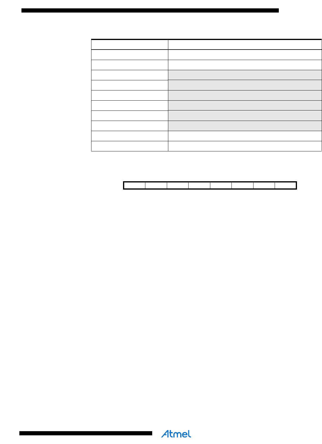
Bit 76543210
ADEN ADSC ADFR ADIF ADIE ADPS2 ADPS1 ADPS0 ADCSRA
Read/Write R/W R/W R/W R/W R/W R/W R/W R/W
Initial Value00000000