
Datasheet


Table Of Contents
- Features
- 1. Pin Configurations
- 2. Overview
- 3. Resources
- 4. Data Retention
- 5. About Code Examples
- 6. Capacitive touch sensing
- 7. AVR CPU Core
- 8. AVR Memories
- 9. System Clock and Clock Options
- 10. Power Management and Sleep Modes
- 11. System Control and Reset
- 12. Interrupts
- 13. I/O Ports
- 13.1 Overview
- 13.2 Ports as General Digital I/O
- 13.3 Alternate Port Functions
- 13.4 Register Description
- 13.4.1 SFIOR – Special Function I/O Register
- 13.4.2 PORTA – Port A Data Register
- 13.4.3 DDRA – Port A Data Direction Register
- 13.4.4 PINA – Port A Input Pins Address
- 13.4.5 PORTB – Port B Data Register
- 13.4.6 DDRB – Port B Data Direction Register
- 13.4.7 PINB – Port B Input Pins Address
- 13.4.8 PORTC – Port C Data Register
- 13.4.9 DDRC – Port C Data Direction Register
- 13.4.10 PINC – Port C Input Pins Address
- 13.4.11 PORTD – Port D Data Register
- 13.4.12 DDRD – Port D Data Direction Register
- 13.4.13 PIND – Port D Input Pins Address
- 14. External Interrupts
- 15. 8-bit Timer/Counter0 with PWM
- 16. Timer/Counter0 and Timer/Counter1 Prescalers
- 17. 16-bit Timer/Counter1
- 17.1 Features
- 17.2 Overview
- 17.3 Accessing 16-bit Registers
- 17.4 Timer/Counter Clock Sources
- 17.5 Counter Unit
- 17.6 Input Capture Unit
- 17.7 Compare Match Output Unit
- 17.8 Modes of Operation
- 17.9 Timer/Counter Timing Diagrams
- 17.10 Register Description
- 17.10.1 TCCR1A – Timer/Counter1 Control Register A
- 17.10.2 TCCR1B – Timer/Counter1 Control Register B
- 17.10.3 TCNT1H and TCNT1L – Timer/Counter1
- 17.10.4 OCR1AH and OCR1AL – Output Compare Register 1 A
- 17.10.5 OCR1BH and OCR1BL – Output Compare Register 1 B
- 17.10.6 ICR1H and ICR1L – Input Capture Register 1
- 17.10.7 TIMSK – Timer/Counter Interrupt Mask Register(1)
- 17.10.8 TIFR – Timer/Counter Interrupt Flag Register
- 18. 8-bit Timer/Counter2 with PWM and Asynchronous Operation
- 18.1 Features
- 18.2 Overview
- 18.3 Timer/Counter Clock Sources
- 18.4 Counter Unit
- 18.5 Output Compare Unit
- 18.6 Compare Match Output Unit
- 18.7 Modes of Operation
- 18.8 Timer/Counter Timing Diagrams
- 18.9 Asynchronous Operation of the Timer/Counter
- 18.10 Timer/Counter Prescaler
- 18.11 Register Description
- 18.11.1 TCCR2 – Timer/Counter Control Register
- 18.11.2 TCNT2 – Timer/Counter Register
- 18.11.3 OCR2 – Output Compare Register
- 18.11.4 ‘ASSR – Asynchronous Status Register
- 18.11.5 TIMSK – Timer/Counter Interrupt Mask Register
- 18.11.6 TIFR – Timer/Counter Interrupt Flag Register
- 18.11.7 SFIOR – Special Function IO Register
- 19. SPI – Serial Peripheral Interface
- 20. USART
- 20.1 Features
- 20.2 Overview
- 20.3 Clock Generation
- 20.4 Frame Formats
- 20.5 USART Initialization
- 20.6 Data Transmission – The USART Transmitter
- 20.7 Data Reception – The USART Receiver
- 20.8 Asynchronous Data Reception
- 20.9 Multi-processor Communication Mode
- 20.10 Accessing UBRRH/ UCSRC Registers
- 20.11 Register Description
- 20.12 Examples of Baud Rate Setting
- 21. Two-wire Serial Interface
- 22. Analog Comparator
- 23. Analog to Digital Converter
- 24. JTAG Interface and On-chip Debug System
- 25. IEEE 1149.1 (JTAG) Boundary-scan
- 26. Boot Loader Support – Read-While-Write Self-Programming
- 26.1 Features
- 26.2 Overview
- 26.3 Application and Boot Loader Flash Sections
- 26.4 Read-While-Write and no Read-While-Write Flash Sections
- 26.5 Boot Loader Lock Bits
- 26.6 Entering the Boot Loader Program
- 26.7 Addressing the Flash during Self-Programming
- 26.8 Self-Programming the Flash
- 26.8.1 Performing Page Erase by SPM
- 26.8.2 Filling the Temporary Buffer (Page Loading)
- 26.8.3 Performing a Page Write
- 26.8.4 Using the SPM Interrupt
- 26.8.5 Consideration while Updating BLS
- 26.8.6 Prevent Reading the RWW Section during Self-Programming
- 26.8.7 Setting the Boot Loader Lock Bits by SPM
- 26.8.8 EEPROM Write Prevents Writing to SPMCR
- 26.8.9 Reading the Fuse and Lock Bits from Software
- 26.8.10 Preventing Flash Corruption
- 26.8.11 Programming Time for Flash when using SPM
- 26.8.12 Simple Assembly Code Example for a Boot Loader
- 26.8.13 Boot Loader Parameters
- 26.9 Register Description
- 27. Memory Programming
- 27.1 Program And Data Memory Lock Bits
- 27.2 Fuse Bits
- 27.3 Signature Bytes
- 27.4 Calibration Byte
- 27.5 Page Size
- 27.6 Parallel Programming Parameters, Pin Mapping, and Commands
- 27.7 Parallel Programming
- 27.7.1 Enter Programming Mode
- 27.7.2 Considerations for Efficient Programming
- 27.7.3 Chip Erase
- 27.7.4 Programming the Flash
- 27.7.5 Programming the EEPROM
- 27.7.6 Reading the Flash
- 27.7.7 Reading the EEPROM
- 27.7.8 Programming the Fuse Low Bits
- 27.7.9 Programming the Fuse High Bits
- 27.7.10 Programming the Lock Bits
- 27.7.11 Reading the Fuse and Lock Bits
- 27.7.12 Reading the Signature Bytes
- 27.7.13 Reading the Calibration Byte
- 27.7.14 Parallel Programming Characteristics
- 27.8 SPI Serial Downloading
- 27.9 SPI Serial Programming Pin Mapping
- 27.10 Programming via the JTAG Interface
- 27.10.1 Programming Specific JTAG Instructions
- 27.10.2 AVR_RESET ($C)
- 27.10.3 PROG_ENABLE ($4)
- 27.10.4 PROG_COMMANDS ($5)
- 27.10.5 PROG_PAGELOAD ($6)
- 27.10.6 PROG_PAGEREAD ($7)
- 27.10.7 Data Registers
- 27.10.8 Reset Register
- 27.10.9 Programming Enable Register
- 27.10.10 Programming Command Register
- 27.10.11 Virtual Flash Page Load Register
- 27.10.12 Virtual Flash Page Read Register
- 27.10.13 Programming Algorithm
- 27.10.14 Entering Programming Mode
- 27.10.15 Leaving Programming Mode
- 27.10.16 Performing Chip Erase
- 27.10.17 Programming the Flash
- 27.10.18 Reading the Flash
- 27.10.19 Programming the EEPROM
- 27.10.20 Reading the EEPROM
- 27.10.21 Programming the Fuses
- 27.10.22 Programming the Lock Bits
- 27.10.23 Reading the Fuses and Lock Bits
- 27.10.24 Reading the Signature Bytes
- 27.10.25 Reading the Calibration Byte
- 28. Electrical Characteristics
- 29. Typical Characteristics
- 29.1 Active Supply Current
- 29.2 Idle Supply Current
- 29.3 Power-down Supply Current
- 29.4 Power-save Supply Current
- 29.5 Standby Supply Current
- 29.6 Pin Pull-up
- 29.7 Pin Driver Strength
- 29.8 Pin Thresholds and Hysteresis
- 29.9 BOD Thresholds and Analog Comparator Offset
- 29.10 Internal Oscillator Speed
- 29.11 Current Consumption of Peripheral Units
- 29.12 Current Consumption in Reset and Reset Pulsewidth
- 30. Register Summary
- 31. Instruction Set Summary
- 32. Ordering Information
- 33. Packaging Information
- 34. Errata
- 35. Datasheet Revision History
- Table of Contents
40
ATmega32A [DATASHEET]
Atmel-8155D-AVR-ATmega32A-Datasheet_02/2014
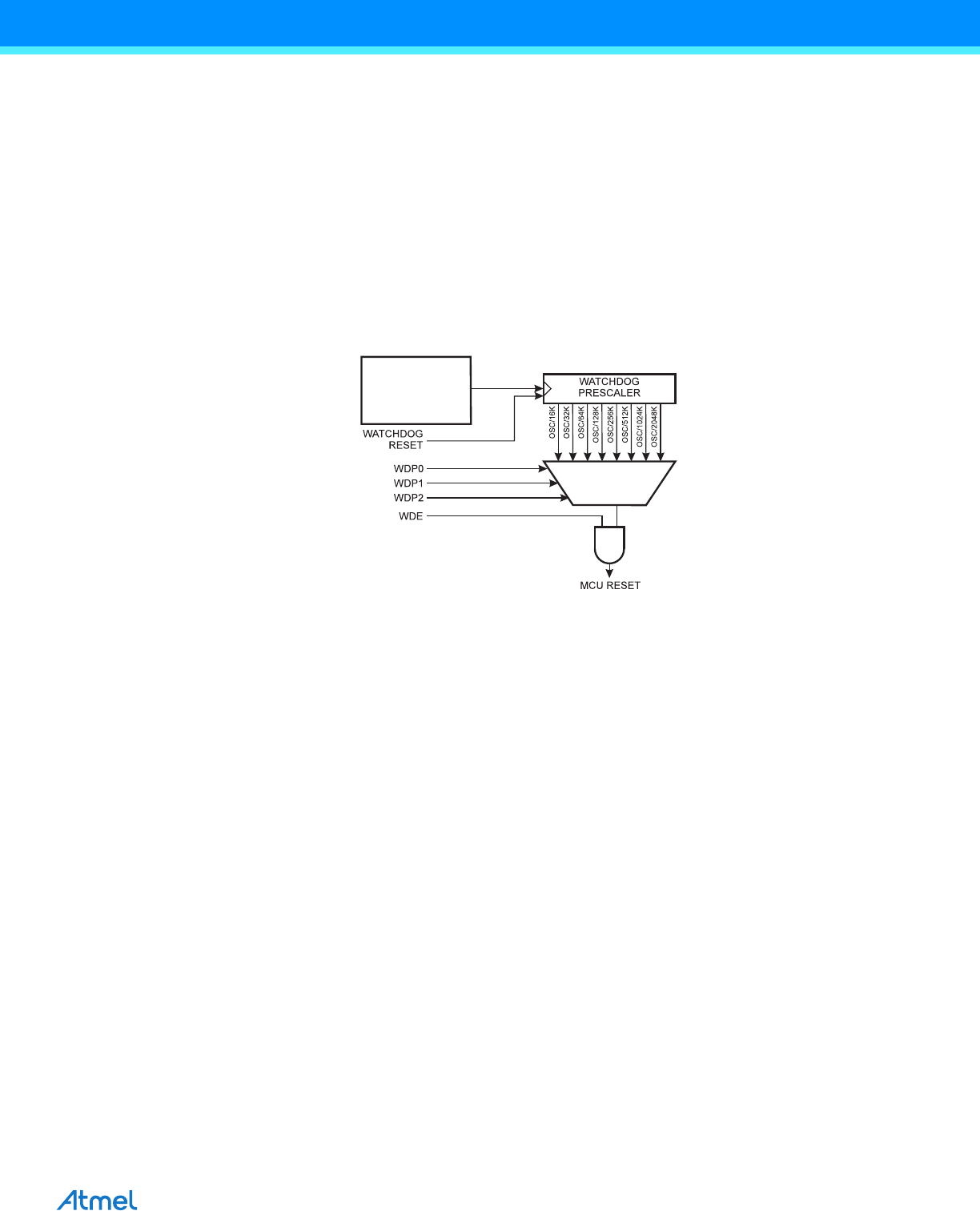
11.4 Watchdog Timer
The Watchdog Timer is clocked from a separate On-chip Oscillator which runs at 1MHz. This is the typical value at
V
CC
= 5V. See characterization data for typical values at other V
CC
levels. By controlling the Watchdog Timer pres-
caler, the Watchdog Reset interval can be adjusted as shown in Table 10-1 on page 44. The WDR – Watchdog
Reset – instruction resets the Watchdog Timer. The Watchdog Timer is also reset when it is disabled and when a
Chip Reset occurs. Eight different clock cycle periods can be selected to determine the reset period. If the reset
period expires without another Watchdog Reset, the ATmega32A resets and executes from the Reset Vector. For
timing details on the Watchdog Reset, refer to page 41.
To prevent unintentional disabling of the Watchdog, a special turn-off sequence must be followed when the Watch-
dog is disabled. Refer to the description of the Watchdog Timer Control Register for details.
Figure 11-7. Watchdog Timer
WATCHDOG
OSCILLATOR