
Datasheet


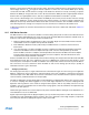
Table Of Contents
- Features
- 1. Pin Configurations
- 2. Overview
- 3. Resources
- 4. Data Retention
- 5. About Code Examples
- 6. Capacitive touch sensing
- 7. AVR CPU Core
- 8. AVR Memories
- 9. System Clock and Clock Options
- 10. Power Management and Sleep Modes
- 11. System Control and Reset
- 12. Interrupts
- 13. I/O Ports
- 13.1 Overview
- 13.2 Ports as General Digital I/O
- 13.3 Alternate Port Functions
- 13.4 Register Description
- 13.4.1 SFIOR – Special Function I/O Register
- 13.4.2 PORTA – Port A Data Register
- 13.4.3 DDRA – Port A Data Direction Register
- 13.4.4 PINA – Port A Input Pins Address
- 13.4.5 PORTB – Port B Data Register
- 13.4.6 DDRB – Port B Data Direction Register
- 13.4.7 PINB – Port B Input Pins Address
- 13.4.8 PORTC – Port C Data Register
- 13.4.9 DDRC – Port C Data Direction Register
- 13.4.10 PINC – Port C Input Pins Address
- 13.4.11 PORTD – Port D Data Register
- 13.4.12 DDRD – Port D Data Direction Register
- 13.4.13 PIND – Port D Input Pins Address
- 14. External Interrupts
- 15. 8-bit Timer/Counter0 with PWM
- 16. Timer/Counter0 and Timer/Counter1 Prescalers
- 17. 16-bit Timer/Counter1
- 17.1 Features
- 17.2 Overview
- 17.3 Accessing 16-bit Registers
- 17.4 Timer/Counter Clock Sources
- 17.5 Counter Unit
- 17.6 Input Capture Unit
- 17.7 Compare Match Output Unit
- 17.8 Modes of Operation
- 17.9 Timer/Counter Timing Diagrams
- 17.10 Register Description
- 17.10.1 TCCR1A – Timer/Counter1 Control Register A
- 17.10.2 TCCR1B – Timer/Counter1 Control Register B
- 17.10.3 TCNT1H and TCNT1L – Timer/Counter1
- 17.10.4 OCR1AH and OCR1AL – Output Compare Register 1 A
- 17.10.5 OCR1BH and OCR1BL – Output Compare Register 1 B
- 17.10.6 ICR1H and ICR1L – Input Capture Register 1
- 17.10.7 TIMSK – Timer/Counter Interrupt Mask Register(1)
- 17.10.8 TIFR – Timer/Counter Interrupt Flag Register
- 18. 8-bit Timer/Counter2 with PWM and Asynchronous Operation
- 18.1 Features
- 18.2 Overview
- 18.3 Timer/Counter Clock Sources
- 18.4 Counter Unit
- 18.5 Output Compare Unit
- 18.6 Compare Match Output Unit
- 18.7 Modes of Operation
- 18.8 Timer/Counter Timing Diagrams
- 18.9 Asynchronous Operation of the Timer/Counter
- 18.10 Timer/Counter Prescaler
- 18.11 Register Description
- 18.11.1 TCCR2 – Timer/Counter Control Register
- 18.11.2 TCNT2 – Timer/Counter Register
- 18.11.3 OCR2 – Output Compare Register
- 18.11.4 ‘ASSR – Asynchronous Status Register
- 18.11.5 TIMSK – Timer/Counter Interrupt Mask Register
- 18.11.6 TIFR – Timer/Counter Interrupt Flag Register
- 18.11.7 SFIOR – Special Function IO Register
- 19. SPI – Serial Peripheral Interface
- 20. USART
- 20.1 Features
- 20.2 Overview
- 20.3 Clock Generation
- 20.4 Frame Formats
- 20.5 USART Initialization
- 20.6 Data Transmission – The USART Transmitter
- 20.7 Data Reception – The USART Receiver
- 20.8 Asynchronous Data Reception
- 20.9 Multi-processor Communication Mode
- 20.10 Accessing UBRRH/ UCSRC Registers
- 20.11 Register Description
- 20.12 Examples of Baud Rate Setting
- 21. Two-wire Serial Interface
- 22. Analog Comparator
- 23. Analog to Digital Converter
- 24. JTAG Interface and On-chip Debug System
- 25. IEEE 1149.1 (JTAG) Boundary-scan
- 26. Boot Loader Support – Read-While-Write Self-Programming
- 26.1 Features
- 26.2 Overview
- 26.3 Application and Boot Loader Flash Sections
- 26.4 Read-While-Write and no Read-While-Write Flash Sections
- 26.5 Boot Loader Lock Bits
- 26.6 Entering the Boot Loader Program
- 26.7 Addressing the Flash during Self-Programming
- 26.8 Self-Programming the Flash
- 26.8.1 Performing Page Erase by SPM
- 26.8.2 Filling the Temporary Buffer (Page Loading)
- 26.8.3 Performing a Page Write
- 26.8.4 Using the SPM Interrupt
- 26.8.5 Consideration while Updating BLS
- 26.8.6 Prevent Reading the RWW Section during Self-Programming
- 26.8.7 Setting the Boot Loader Lock Bits by SPM
- 26.8.8 EEPROM Write Prevents Writing to SPMCR
- 26.8.9 Reading the Fuse and Lock Bits from Software
- 26.8.10 Preventing Flash Corruption
- 26.8.11 Programming Time for Flash when using SPM
- 26.8.12 Simple Assembly Code Example for a Boot Loader
- 26.8.13 Boot Loader Parameters
- 26.9 Register Description
- 27. Memory Programming
- 27.1 Program And Data Memory Lock Bits
- 27.2 Fuse Bits
- 27.3 Signature Bytes
- 27.4 Calibration Byte
- 27.5 Page Size
- 27.6 Parallel Programming Parameters, Pin Mapping, and Commands
- 27.7 Parallel Programming
- 27.7.1 Enter Programming Mode
- 27.7.2 Considerations for Efficient Programming
- 27.7.3 Chip Erase
- 27.7.4 Programming the Flash
- 27.7.5 Programming the EEPROM
- 27.7.6 Reading the Flash
- 27.7.7 Reading the EEPROM
- 27.7.8 Programming the Fuse Low Bits
- 27.7.9 Programming the Fuse High Bits
- 27.7.10 Programming the Lock Bits
- 27.7.11 Reading the Fuse and Lock Bits
- 27.7.12 Reading the Signature Bytes
- 27.7.13 Reading the Calibration Byte
- 27.7.14 Parallel Programming Characteristics
- 27.8 SPI Serial Downloading
- 27.9 SPI Serial Programming Pin Mapping
- 27.10 Programming via the JTAG Interface
- 27.10.1 Programming Specific JTAG Instructions
- 27.10.2 AVR_RESET ($C)
- 27.10.3 PROG_ENABLE ($4)
- 27.10.4 PROG_COMMANDS ($5)
- 27.10.5 PROG_PAGELOAD ($6)
- 27.10.6 PROG_PAGEREAD ($7)
- 27.10.7 Data Registers
- 27.10.8 Reset Register
- 27.10.9 Programming Enable Register
- 27.10.10 Programming Command Register
- 27.10.11 Virtual Flash Page Load Register
- 27.10.12 Virtual Flash Page Read Register
- 27.10.13 Programming Algorithm
- 27.10.14 Entering Programming Mode
- 27.10.15 Leaving Programming Mode
- 27.10.16 Performing Chip Erase
- 27.10.17 Programming the Flash
- 27.10.18 Reading the Flash
- 27.10.19 Programming the EEPROM
- 27.10.20 Reading the EEPROM
- 27.10.21 Programming the Fuses
- 27.10.22 Programming the Lock Bits
- 27.10.23 Reading the Fuses and Lock Bits
- 27.10.24 Reading the Signature Bytes
- 27.10.25 Reading the Calibration Byte
- 28. Electrical Characteristics
- 29. Typical Characteristics
- 29.1 Active Supply Current
- 29.2 Idle Supply Current
- 29.3 Power-down Supply Current
- 29.4 Power-save Supply Current
- 29.5 Standby Supply Current
- 29.6 Pin Pull-up
- 29.7 Pin Driver Strength
- 29.8 Pin Thresholds and Hysteresis
- 29.9 BOD Thresholds and Analog Comparator Offset
- 29.10 Internal Oscillator Speed
- 29.11 Current Consumption of Peripheral Units
- 29.12 Current Consumption in Reset and Reset Pulsewidth
- 30. Register Summary
- 31. Instruction Set Summary
- 32. Ordering Information
- 33. Packaging Information
- 34. Errata
- 35. Datasheet Revision History
- Table of Contents

198
ATmega32A [DATASHEET]
Atmel-8155D-AVR-ATmega32A-Datasheet_02/2014
Figure 23-7. ADC Timing Diagram, Free Running Conversion
23.5.1 Differential Gain Channels
When using differential gain channels, certain aspects of the conversion need to be taken into consideration.
Differential conversions are synchronized to the internal clock CK
ADC2
equal to half the ADC clock. This synchroni-
zation is done automatically by the ADC interface in such a way that the sample-and-hold occurs at a specific
phase of CK
ADC2
. A conversion initiated by the user (that is, all single conversions, and the first free running con-
version) when CK
ADC2
is low will take the same amount of time as a single ended conversion (13 ADC clock cycles
from the next prescaled clock cycle). A conversion initiated by the user when CK
ADC2
is high will take 14 ADC clock
cycles due to the synchronization mechanism. In Free Running mode, a new conversion is initiated immediately
after the previous conversion completes, and since CK
ADC2
is high at this time, all automatically started (that is, all
but the first) free running conversions will take 14 ADC clock cycles.
The gain stage is optimized for a bandwidth of 4kHz at all gain settings. Higher frequencies may be subjected to
non-linear amplification. An external low-pass filter should be used if the input signal contains higher frequency
components than the gain stage bandwidth. Note that the ADC clock frequency is independent of the gain stage
bandwidth limitation. For example, the ADC clock period may be 6 µs, allowing a channel to be sampled at
12kSPS, regardless of the bandwidth of this channel.
If differential gain channels are used and conversions are started by Auto Triggering, the ADC must be switched off
between conversions. When Auto Triggering is used, the ADC prescaler is reset before the conversion is started.
Since the gain stage is dependent of a stable ADC clock prior to the conversion, this conversion will not be valid.
By disabling and then re-enabling the ADC between each conversion (writing ADEN in ADCSRA to “0” then to “1”),
only extended conversions are performed. The result from the extended conversions will be valid. See “Prescaling
and Conversion Timing” on page 211 for timing details.
Table 23-1. ADC Conversion Time
Condition
Sample & Hold (Cycles
from Start of Conversion) Conversion Time (Cycles)
First conversion 13.5 25
Normal conversions, single ended 1.5 13
Auto Triggered conversions 2 13.5
Normal conversions, differential 1.5/2.5 13/14
11 12 13
MSB of Result
LSB of Result
ADC Clock
ADSC
ADIF
ADCH
ADCL
Cycle Number
12
One Conversion Next Conversion
34
Conversion
Complete
Sample & Hold
MUX and REFS
Update