
Datasheet


Table Of Contents
- Features
- 1. Pin Configurations
- 2. Overview
- 3. Resources
- 4. Data Retention
- 5. About Code Examples
- 6. Capacitive touch sensing
- 7. AVR CPU Core
- 8. AVR Memories
- 9. System Clock and Clock Options
- 10. Power Management and Sleep Modes
- 11. System Control and Reset
- 12. Interrupts
- 13. I/O Ports
- 13.1 Overview
- 13.2 Ports as General Digital I/O
- 13.3 Alternate Port Functions
- 13.4 Register Description
- 13.4.1 SFIOR – Special Function I/O Register
- 13.4.2 PORTA – Port A Data Register
- 13.4.3 DDRA – Port A Data Direction Register
- 13.4.4 PINA – Port A Input Pins Address
- 13.4.5 PORTB – Port B Data Register
- 13.4.6 DDRB – Port B Data Direction Register
- 13.4.7 PINB – Port B Input Pins Address
- 13.4.8 PORTC – Port C Data Register
- 13.4.9 DDRC – Port C Data Direction Register
- 13.4.10 PINC – Port C Input Pins Address
- 13.4.11 PORTD – Port D Data Register
- 13.4.12 DDRD – Port D Data Direction Register
- 13.4.13 PIND – Port D Input Pins Address
- 14. External Interrupts
- 15. 8-bit Timer/Counter0 with PWM
- 16. Timer/Counter0 and Timer/Counter1 Prescalers
- 17. 16-bit Timer/Counter1
- 17.1 Features
- 17.2 Overview
- 17.3 Accessing 16-bit Registers
- 17.4 Timer/Counter Clock Sources
- 17.5 Counter Unit
- 17.6 Input Capture Unit
- 17.7 Compare Match Output Unit
- 17.8 Modes of Operation
- 17.9 Timer/Counter Timing Diagrams
- 17.10 Register Description
- 17.10.1 TCCR1A – Timer/Counter1 Control Register A
- 17.10.2 TCCR1B – Timer/Counter1 Control Register B
- 17.10.3 TCNT1H and TCNT1L – Timer/Counter1
- 17.10.4 OCR1AH and OCR1AL – Output Compare Register 1 A
- 17.10.5 OCR1BH and OCR1BL – Output Compare Register 1 B
- 17.10.6 ICR1H and ICR1L – Input Capture Register 1
- 17.10.7 TIMSK – Timer/Counter Interrupt Mask Register(1)
- 17.10.8 TIFR – Timer/Counter Interrupt Flag Register
- 18. 8-bit Timer/Counter2 with PWM and Asynchronous Operation
- 18.1 Features
- 18.2 Overview
- 18.3 Timer/Counter Clock Sources
- 18.4 Counter Unit
- 18.5 Output Compare Unit
- 18.6 Compare Match Output Unit
- 18.7 Modes of Operation
- 18.8 Timer/Counter Timing Diagrams
- 18.9 Asynchronous Operation of the Timer/Counter
- 18.10 Timer/Counter Prescaler
- 18.11 Register Description
- 18.11.1 TCCR2 – Timer/Counter Control Register
- 18.11.2 TCNT2 – Timer/Counter Register
- 18.11.3 OCR2 – Output Compare Register
- 18.11.4 ‘ASSR – Asynchronous Status Register
- 18.11.5 TIMSK – Timer/Counter Interrupt Mask Register
- 18.11.6 TIFR – Timer/Counter Interrupt Flag Register
- 18.11.7 SFIOR – Special Function IO Register
- 19. SPI – Serial Peripheral Interface
- 20. USART
- 20.1 Features
- 20.2 Overview
- 20.3 Clock Generation
- 20.4 Frame Formats
- 20.5 USART Initialization
- 20.6 Data Transmission – The USART Transmitter
- 20.7 Data Reception – The USART Receiver
- 20.8 Asynchronous Data Reception
- 20.9 Multi-processor Communication Mode
- 20.10 Accessing UBRRH/ UCSRC Registers
- 20.11 Register Description
- 20.12 Examples of Baud Rate Setting
- 21. Two-wire Serial Interface
- 22. Analog Comparator
- 23. Analog to Digital Converter
- 24. JTAG Interface and On-chip Debug System
- 25. IEEE 1149.1 (JTAG) Boundary-scan
- 26. Boot Loader Support – Read-While-Write Self-Programming
- 26.1 Features
- 26.2 Overview
- 26.3 Application and Boot Loader Flash Sections
- 26.4 Read-While-Write and no Read-While-Write Flash Sections
- 26.5 Boot Loader Lock Bits
- 26.6 Entering the Boot Loader Program
- 26.7 Addressing the Flash during Self-Programming
- 26.8 Self-Programming the Flash
- 26.8.1 Performing Page Erase by SPM
- 26.8.2 Filling the Temporary Buffer (Page Loading)
- 26.8.3 Performing a Page Write
- 26.8.4 Using the SPM Interrupt
- 26.8.5 Consideration while Updating BLS
- 26.8.6 Prevent Reading the RWW Section during Self-Programming
- 26.8.7 Setting the Boot Loader Lock Bits by SPM
- 26.8.8 EEPROM Write Prevents Writing to SPMCR
- 26.8.9 Reading the Fuse and Lock Bits from Software
- 26.8.10 Preventing Flash Corruption
- 26.8.11 Programming Time for Flash when using SPM
- 26.8.12 Simple Assembly Code Example for a Boot Loader
- 26.8.13 Boot Loader Parameters
- 26.9 Register Description
- 27. Memory Programming
- 27.1 Program And Data Memory Lock Bits
- 27.2 Fuse Bits
- 27.3 Signature Bytes
- 27.4 Calibration Byte
- 27.5 Page Size
- 27.6 Parallel Programming Parameters, Pin Mapping, and Commands
- 27.7 Parallel Programming
- 27.7.1 Enter Programming Mode
- 27.7.2 Considerations for Efficient Programming
- 27.7.3 Chip Erase
- 27.7.4 Programming the Flash
- 27.7.5 Programming the EEPROM
- 27.7.6 Reading the Flash
- 27.7.7 Reading the EEPROM
- 27.7.8 Programming the Fuse Low Bits
- 27.7.9 Programming the Fuse High Bits
- 27.7.10 Programming the Lock Bits
- 27.7.11 Reading the Fuse and Lock Bits
- 27.7.12 Reading the Signature Bytes
- 27.7.13 Reading the Calibration Byte
- 27.7.14 Parallel Programming Characteristics
- 27.8 SPI Serial Downloading
- 27.9 SPI Serial Programming Pin Mapping
- 27.10 Programming via the JTAG Interface
- 27.10.1 Programming Specific JTAG Instructions
- 27.10.2 AVR_RESET ($C)
- 27.10.3 PROG_ENABLE ($4)
- 27.10.4 PROG_COMMANDS ($5)
- 27.10.5 PROG_PAGELOAD ($6)
- 27.10.6 PROG_PAGEREAD ($7)
- 27.10.7 Data Registers
- 27.10.8 Reset Register
- 27.10.9 Programming Enable Register
- 27.10.10 Programming Command Register
- 27.10.11 Virtual Flash Page Load Register
- 27.10.12 Virtual Flash Page Read Register
- 27.10.13 Programming Algorithm
- 27.10.14 Entering Programming Mode
- 27.10.15 Leaving Programming Mode
- 27.10.16 Performing Chip Erase
- 27.10.17 Programming the Flash
- 27.10.18 Reading the Flash
- 27.10.19 Programming the EEPROM
- 27.10.20 Reading the EEPROM
- 27.10.21 Programming the Fuses
- 27.10.22 Programming the Lock Bits
- 27.10.23 Reading the Fuses and Lock Bits
- 27.10.24 Reading the Signature Bytes
- 27.10.25 Reading the Calibration Byte
- 28. Electrical Characteristics
- 29. Typical Characteristics
- 29.1 Active Supply Current
- 29.2 Idle Supply Current
- 29.3 Power-down Supply Current
- 29.4 Power-save Supply Current
- 29.5 Standby Supply Current
- 29.6 Pin Pull-up
- 29.7 Pin Driver Strength
- 29.8 Pin Thresholds and Hysteresis
- 29.9 BOD Thresholds and Analog Comparator Offset
- 29.10 Internal Oscillator Speed
- 29.11 Current Consumption of Peripheral Units
- 29.12 Current Consumption in Reset and Reset Pulsewidth
- 30. Register Summary
- 31. Instruction Set Summary
- 32. Ordering Information
- 33. Packaging Information
- 34. Errata
- 35. Datasheet Revision History
- Table of Contents
166
ATmega32A [DATASHEET]
Atmel-8155D-AVR-ATmega32A-Datasheet_02/2014
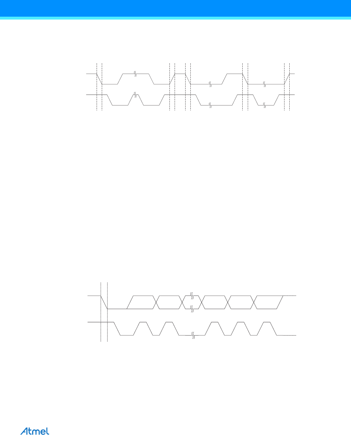
for the remainder of this datasheet, unless otherwise noted. As depicted below, START and STOP conditions are
signalled by changing the level of the SDA line when the SCL line is high.
Figure 21-3. START, REPEATED START, and STOP Conditions
21.3.3 Address Packet Format
All address packets transmitted on the TWI bus are nine bits long, consisting of seven address bits, one
READ/WRITE control bit and an acknowledge bit. If the READ/WRITE bit is set, a read operation is to be per-
formed, otherwise a write operation should be performed. When a slave recognizes that it is being addressed, it
should acknowledge by pulling SDA low in the ninth SCL (ACK) cycle. If the addressed slave is busy, or for some
other reason can not service the master’s request, the SDA line should be left high in the ACK clock cycle. The
master can then transmit a STOP condition, or a REPEATED START condition to initiate a new transmission. An
address packet consisting of a slave address and a READ or a WRITE bit is called SLA+R or SLA+W, respectively.
The MSB of the address byte is transmitted first. Slave addresses can freely be allocated by the designer, but the
address 0000 000 is reserved for a general call.
When a general call is issued, all slaves should respond by pulling the SDA line low in the ACK cycle. A general
call is used when a master wishes to transmit the same message to several slaves in the system. When the gen-
eral call address followed by a Write bit is transmitted on the bus, all slaves set up to acknowledge the general call
will pull the SDA line low in the ack cycle. The following data packets will then be received by all the slaves that
acknowledged the general call. Note that transmitting the general call address followed by a Read bit is meaning-
less, as this would cause contention if several slaves started transmitting different data.
All addresses of the format 1111 xxx should be reserved for future purposes.
Figure 21-4. Address Packet Format
21.3.4 Data Packet Format
All data packets transmitted on the TWI bus are nine bits long, consisting of one data byte and an acknowledge bit.
During a data transfer, the master generates the clock and the START and STOP conditions, while the receiver is
responsible for acknowledging the reception. An Acknowledge (ACK) is signalled by the receiver pulling the SDA
line low during the ninth SCL cycle. If the receiver leaves the SDA line high, a NACK is signalled. When the
receiver has received the last byte, or for some reason cannot receive any more bytes, it should inform the trans-
mitter by sending a NACK after the final byte. The MSB of the data byte is transmitted first.
SDA
SCL
START STOPREPEATED START
STOP START
SDA
SCL
START
12 789
Addr MSB Addr LSB R/W
ACK