
Datasheet


Table Of Contents
- Features
- 1. Pin Configurations
- 2. Overview
- 3. Resources
- 4. Data Retention
- 5. About Code Examples
- 6. Capacitive touch sensing
- 7. AVR CPU Core
- 8. AVR Memories
- 9. System Clock and Clock Options
- 10. Power Management and Sleep Modes
- 11. System Control and Reset
- 12. Interrupts
- 13. I/O Ports
- 13.1 Overview
- 13.2 Ports as General Digital I/O
- 13.3 Alternate Port Functions
- 13.4 Register Description
- 13.4.1 SFIOR – Special Function I/O Register
- 13.4.2 PORTA – Port A Data Register
- 13.4.3 DDRA – Port A Data Direction Register
- 13.4.4 PINA – Port A Input Pins Address
- 13.4.5 PORTB – Port B Data Register
- 13.4.6 DDRB – Port B Data Direction Register
- 13.4.7 PINB – Port B Input Pins Address
- 13.4.8 PORTC – Port C Data Register
- 13.4.9 DDRC – Port C Data Direction Register
- 13.4.10 PINC – Port C Input Pins Address
- 13.4.11 PORTD – Port D Data Register
- 13.4.12 DDRD – Port D Data Direction Register
- 13.4.13 PIND – Port D Input Pins Address
- 14. External Interrupts
- 15. 8-bit Timer/Counter0 with PWM
- 16. Timer/Counter0 and Timer/Counter1 Prescalers
- 17. 16-bit Timer/Counter1
- 17.1 Features
- 17.2 Overview
- 17.3 Accessing 16-bit Registers
- 17.4 Timer/Counter Clock Sources
- 17.5 Counter Unit
- 17.6 Input Capture Unit
- 17.7 Compare Match Output Unit
- 17.8 Modes of Operation
- 17.9 Timer/Counter Timing Diagrams
- 17.10 Register Description
- 17.10.1 TCCR1A – Timer/Counter1 Control Register A
- 17.10.2 TCCR1B – Timer/Counter1 Control Register B
- 17.10.3 TCNT1H and TCNT1L – Timer/Counter1
- 17.10.4 OCR1AH and OCR1AL – Output Compare Register 1 A
- 17.10.5 OCR1BH and OCR1BL – Output Compare Register 1 B
- 17.10.6 ICR1H and ICR1L – Input Capture Register 1
- 17.10.7 TIMSK – Timer/Counter Interrupt Mask Register(1)
- 17.10.8 TIFR – Timer/Counter Interrupt Flag Register
- 18. 8-bit Timer/Counter2 with PWM and Asynchronous Operation
- 18.1 Features
- 18.2 Overview
- 18.3 Timer/Counter Clock Sources
- 18.4 Counter Unit
- 18.5 Output Compare Unit
- 18.6 Compare Match Output Unit
- 18.7 Modes of Operation
- 18.8 Timer/Counter Timing Diagrams
- 18.9 Asynchronous Operation of the Timer/Counter
- 18.10 Timer/Counter Prescaler
- 18.11 Register Description
- 18.11.1 TCCR2 – Timer/Counter Control Register
- 18.11.2 TCNT2 – Timer/Counter Register
- 18.11.3 OCR2 – Output Compare Register
- 18.11.4 ‘ASSR – Asynchronous Status Register
- 18.11.5 TIMSK – Timer/Counter Interrupt Mask Register
- 18.11.6 TIFR – Timer/Counter Interrupt Flag Register
- 18.11.7 SFIOR – Special Function IO Register
- 19. SPI – Serial Peripheral Interface
- 20. USART
- 20.1 Features
- 20.2 Overview
- 20.3 Clock Generation
- 20.4 Frame Formats
- 20.5 USART Initialization
- 20.6 Data Transmission – The USART Transmitter
- 20.7 Data Reception – The USART Receiver
- 20.8 Asynchronous Data Reception
- 20.9 Multi-processor Communication Mode
- 20.10 Accessing UBRRH/ UCSRC Registers
- 20.11 Register Description
- 20.12 Examples of Baud Rate Setting
- 21. Two-wire Serial Interface
- 22. Analog Comparator
- 23. Analog to Digital Converter
- 24. JTAG Interface and On-chip Debug System
- 25. IEEE 1149.1 (JTAG) Boundary-scan
- 26. Boot Loader Support – Read-While-Write Self-Programming
- 26.1 Features
- 26.2 Overview
- 26.3 Application and Boot Loader Flash Sections
- 26.4 Read-While-Write and no Read-While-Write Flash Sections
- 26.5 Boot Loader Lock Bits
- 26.6 Entering the Boot Loader Program
- 26.7 Addressing the Flash during Self-Programming
- 26.8 Self-Programming the Flash
- 26.8.1 Performing Page Erase by SPM
- 26.8.2 Filling the Temporary Buffer (Page Loading)
- 26.8.3 Performing a Page Write
- 26.8.4 Using the SPM Interrupt
- 26.8.5 Consideration while Updating BLS
- 26.8.6 Prevent Reading the RWW Section during Self-Programming
- 26.8.7 Setting the Boot Loader Lock Bits by SPM
- 26.8.8 EEPROM Write Prevents Writing to SPMCR
- 26.8.9 Reading the Fuse and Lock Bits from Software
- 26.8.10 Preventing Flash Corruption
- 26.8.11 Programming Time for Flash when using SPM
- 26.8.12 Simple Assembly Code Example for a Boot Loader
- 26.8.13 Boot Loader Parameters
- 26.9 Register Description
- 27. Memory Programming
- 27.1 Program And Data Memory Lock Bits
- 27.2 Fuse Bits
- 27.3 Signature Bytes
- 27.4 Calibration Byte
- 27.5 Page Size
- 27.6 Parallel Programming Parameters, Pin Mapping, and Commands
- 27.7 Parallel Programming
- 27.7.1 Enter Programming Mode
- 27.7.2 Considerations for Efficient Programming
- 27.7.3 Chip Erase
- 27.7.4 Programming the Flash
- 27.7.5 Programming the EEPROM
- 27.7.6 Reading the Flash
- 27.7.7 Reading the EEPROM
- 27.7.8 Programming the Fuse Low Bits
- 27.7.9 Programming the Fuse High Bits
- 27.7.10 Programming the Lock Bits
- 27.7.11 Reading the Fuse and Lock Bits
- 27.7.12 Reading the Signature Bytes
- 27.7.13 Reading the Calibration Byte
- 27.7.14 Parallel Programming Characteristics
- 27.8 SPI Serial Downloading
- 27.9 SPI Serial Programming Pin Mapping
- 27.10 Programming via the JTAG Interface
- 27.10.1 Programming Specific JTAG Instructions
- 27.10.2 AVR_RESET ($C)
- 27.10.3 PROG_ENABLE ($4)
- 27.10.4 PROG_COMMANDS ($5)
- 27.10.5 PROG_PAGELOAD ($6)
- 27.10.6 PROG_PAGEREAD ($7)
- 27.10.7 Data Registers
- 27.10.8 Reset Register
- 27.10.9 Programming Enable Register
- 27.10.10 Programming Command Register
- 27.10.11 Virtual Flash Page Load Register
- 27.10.12 Virtual Flash Page Read Register
- 27.10.13 Programming Algorithm
- 27.10.14 Entering Programming Mode
- 27.10.15 Leaving Programming Mode
- 27.10.16 Performing Chip Erase
- 27.10.17 Programming the Flash
- 27.10.18 Reading the Flash
- 27.10.19 Programming the EEPROM
- 27.10.20 Reading the EEPROM
- 27.10.21 Programming the Fuses
- 27.10.22 Programming the Lock Bits
- 27.10.23 Reading the Fuses and Lock Bits
- 27.10.24 Reading the Signature Bytes
- 27.10.25 Reading the Calibration Byte
- 28. Electrical Characteristics
- 29. Typical Characteristics
- 29.1 Active Supply Current
- 29.2 Idle Supply Current
- 29.3 Power-down Supply Current
- 29.4 Power-save Supply Current
- 29.5 Standby Supply Current
- 29.6 Pin Pull-up
- 29.7 Pin Driver Strength
- 29.8 Pin Thresholds and Hysteresis
- 29.9 BOD Thresholds and Analog Comparator Offset
- 29.10 Internal Oscillator Speed
- 29.11 Current Consumption of Peripheral Units
- 29.12 Current Consumption in Reset and Reset Pulsewidth
- 30. Register Summary
- 31. Instruction Set Summary
- 32. Ordering Information
- 33. Packaging Information
- 34. Errata
- 35. Datasheet Revision History
- Table of Contents
115
ATmega32A [DATASHEET]
Atmel-8155D-AVR-ATmega32A-Datasheet_02/2014
Be aware that the COM2[1:0] bits are not double buffered together with the compare value. Changing the
COM2[1:0] bits will take effect immediately.
18.6 Compare Match Output Unit
The Compare Output mode (COM21:0) bits have two functions. The Waveform Generator uses the COM2[1:0] bits
for defining the Output Compare (OC2) state at the next compare match. Also, the COM2[1:0] bits control the OC2
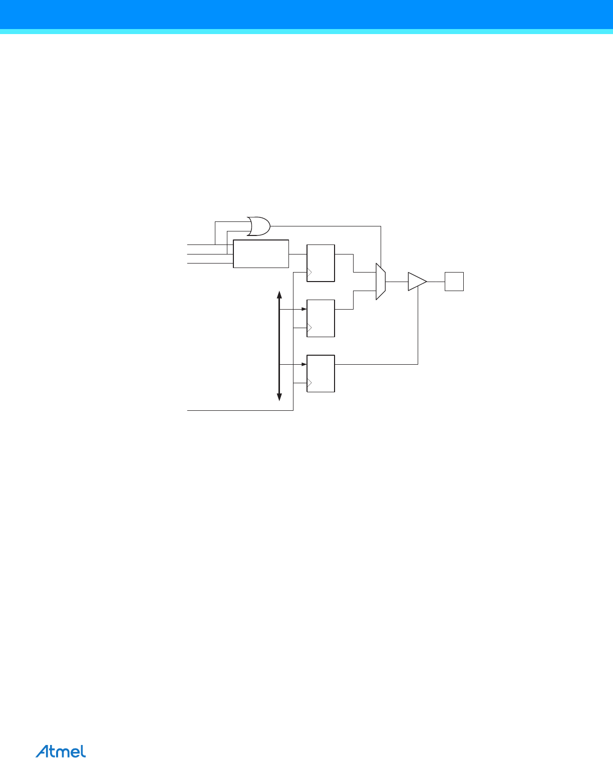
pin output source. Figure 17-4 shows a simplified schematic of the logic affected by the COM2[1:0] bit setting. The
I/O Registers, I/O bits, and I/O pins in the figure are shown in bold. Only the parts of the general I/O Port Control
Registers (DDR and PORT) that are affected by the COM2[1:0] bits are shown. When referring to the OC2 state,
the reference is for the internal OC2 Register, not the OC2 pin.
Figure 18-4. Compare Match Output Unit, Schematic
The general I/O port function is overridden by the Output Compare (OC2) from the waveform generator if either of
the COM2[1:0] bits are set. However, the OC2 pin direction (input or output) is still controlled by the Data Direction
Register (DDR) for the port pin. The Data Direction Register bit for the OC2 pin (DDR_OC2) must be set as output
before the OC2 value is visible on the pin. The port override function is independent of the Waveform Generation
mode.
The design of the output compare pin logic allows initialization of the OC2 state before the output is enabled. Note
that some COM2[1:0] bit settings are reserved for certain modes of operation. “Register Description” on page 132
18.6.1 Compare Output Mode and Waveform Generation
The waveform generator uses the COM2[1:0] bits differently in Normal, CTC, and PWM modes. For all modes, set-
ting the COM2[1:0] = 0 tells the Waveform Generator that no action on the OC2 Register is to be performed on the
next compare match. For compare output actions in the non-PWM modes refer to Table 17-3 on page 133. For fast
PWM mode, refer to Table 17-4 on page 134, and for phase correct PWM refer to Table 17-5 on page 134.
A change of the COM21:0 bits state will have effect at the first compare match after the bits are written. For non-
PWM modes, the action can be forced to have immediate effect by using the FOC2 strobe bits.
18.7 Modes of Operation
The mode of operation, that is, the behavior of the Timer/Counter and the output compare pins, is defined by the
combination of the Waveform Generation mode (WGM2[1:0]) and Compare Output mode (COM2[1:0]) bits. The
Compare Output mode bits do not affect the counting sequence, while the Waveform Generation mode bits do.
The COM2[1:0] bits control whether the PWM output generated should be inverted or not (inverted or non-inverted
PORT
DDR
DQ
DQ
OCn
Pin
OCn
DQ
Waveform
Generator
COMn1
COMn0
0
1
DATA BU S
FOCn
clk
I/O