
Datasheet


Table Of Contents
- Features
- 1. Pin Configurations
- 2. Overview
- 3. Resources
- 4. Data Retention
- 5. About Code Examples
- 6. Capacitive touch sensing
- 7. AVR CPU Core
- 8. AVR Memories
- 9. System Clock and Clock Options
- 10. Power Management and Sleep Modes
- 11. System Control and Reset
- 12. Interrupts
- 13. I/O Ports
- 13.1 Overview
- 13.2 Ports as General Digital I/O
- 13.3 Alternate Port Functions
- 13.4 Register Description
- 13.4.1 SFIOR – Special Function I/O Register
- 13.4.2 PORTA – Port A Data Register
- 13.4.3 DDRA – Port A Data Direction Register
- 13.4.4 PINA – Port A Input Pins Address
- 13.4.5 PORTB – Port B Data Register
- 13.4.6 DDRB – Port B Data Direction Register
- 13.4.7 PINB – Port B Input Pins Address
- 13.4.8 PORTC – Port C Data Register
- 13.4.9 DDRC – Port C Data Direction Register
- 13.4.10 PINC – Port C Input Pins Address
- 13.4.11 PORTD – Port D Data Register
- 13.4.12 DDRD – Port D Data Direction Register
- 13.4.13 PIND – Port D Input Pins Address
- 14. External Interrupts
- 15. 8-bit Timer/Counter0 with PWM
- 16. Timer/Counter0 and Timer/Counter1 Prescalers
- 17. 16-bit Timer/Counter1
- 17.1 Features
- 17.2 Overview
- 17.3 Accessing 16-bit Registers
- 17.4 Timer/Counter Clock Sources
- 17.5 Counter Unit
- 17.6 Input Capture Unit
- 17.7 Compare Match Output Unit
- 17.8 Modes of Operation
- 17.9 Timer/Counter Timing Diagrams
- 17.10 Register Description
- 17.10.1 TCCR1A – Timer/Counter1 Control Register A
- 17.10.2 TCCR1B – Timer/Counter1 Control Register B
- 17.10.3 TCNT1H and TCNT1L – Timer/Counter1
- 17.10.4 OCR1AH and OCR1AL – Output Compare Register 1 A
- 17.10.5 OCR1BH and OCR1BL – Output Compare Register 1 B
- 17.10.6 ICR1H and ICR1L – Input Capture Register 1
- 17.10.7 TIMSK – Timer/Counter Interrupt Mask Register(1)
- 17.10.8 TIFR – Timer/Counter Interrupt Flag Register
- 18. 8-bit Timer/Counter2 with PWM and Asynchronous Operation
- 18.1 Features
- 18.2 Overview
- 18.3 Timer/Counter Clock Sources
- 18.4 Counter Unit
- 18.5 Output Compare Unit
- 18.6 Compare Match Output Unit
- 18.7 Modes of Operation
- 18.8 Timer/Counter Timing Diagrams
- 18.9 Asynchronous Operation of the Timer/Counter
- 18.10 Timer/Counter Prescaler
- 18.11 Register Description
- 18.11.1 TCCR2 – Timer/Counter Control Register
- 18.11.2 TCNT2 – Timer/Counter Register
- 18.11.3 OCR2 – Output Compare Register
- 18.11.4 ‘ASSR – Asynchronous Status Register
- 18.11.5 TIMSK – Timer/Counter Interrupt Mask Register
- 18.11.6 TIFR – Timer/Counter Interrupt Flag Register
- 18.11.7 SFIOR – Special Function IO Register
- 19. SPI – Serial Peripheral Interface
- 20. USART
- 20.1 Features
- 20.2 Overview
- 20.3 Clock Generation
- 20.4 Frame Formats
- 20.5 USART Initialization
- 20.6 Data Transmission – The USART Transmitter
- 20.7 Data Reception – The USART Receiver
- 20.8 Asynchronous Data Reception
- 20.9 Multi-processor Communication Mode
- 20.10 Accessing UBRRH/ UCSRC Registers
- 20.11 Register Description
- 20.12 Examples of Baud Rate Setting
- 21. Two-wire Serial Interface
- 22. Analog Comparator
- 23. Analog to Digital Converter
- 24. JTAG Interface and On-chip Debug System
- 25. IEEE 1149.1 (JTAG) Boundary-scan
- 26. Boot Loader Support – Read-While-Write Self-Programming
- 26.1 Features
- 26.2 Overview
- 26.3 Application and Boot Loader Flash Sections
- 26.4 Read-While-Write and no Read-While-Write Flash Sections
- 26.5 Boot Loader Lock Bits
- 26.6 Entering the Boot Loader Program
- 26.7 Addressing the Flash during Self-Programming
- 26.8 Self-Programming the Flash
- 26.8.1 Performing Page Erase by SPM
- 26.8.2 Filling the Temporary Buffer (Page Loading)
- 26.8.3 Performing a Page Write
- 26.8.4 Using the SPM Interrupt
- 26.8.5 Consideration while Updating BLS
- 26.8.6 Prevent Reading the RWW Section during Self-Programming
- 26.8.7 Setting the Boot Loader Lock Bits by SPM
- 26.8.8 EEPROM Write Prevents Writing to SPMCR
- 26.8.9 Reading the Fuse and Lock Bits from Software
- 26.8.10 Preventing Flash Corruption
- 26.8.11 Programming Time for Flash when using SPM
- 26.8.12 Simple Assembly Code Example for a Boot Loader
- 26.8.13 Boot Loader Parameters
- 26.9 Register Description
- 27. Memory Programming
- 27.1 Program And Data Memory Lock Bits
- 27.2 Fuse Bits
- 27.3 Signature Bytes
- 27.4 Calibration Byte
- 27.5 Page Size
- 27.6 Parallel Programming Parameters, Pin Mapping, and Commands
- 27.7 Parallel Programming
- 27.7.1 Enter Programming Mode
- 27.7.2 Considerations for Efficient Programming
- 27.7.3 Chip Erase
- 27.7.4 Programming the Flash
- 27.7.5 Programming the EEPROM
- 27.7.6 Reading the Flash
- 27.7.7 Reading the EEPROM
- 27.7.8 Programming the Fuse Low Bits
- 27.7.9 Programming the Fuse High Bits
- 27.7.10 Programming the Lock Bits
- 27.7.11 Reading the Fuse and Lock Bits
- 27.7.12 Reading the Signature Bytes
- 27.7.13 Reading the Calibration Byte
- 27.7.14 Parallel Programming Characteristics
- 27.8 SPI Serial Downloading
- 27.9 SPI Serial Programming Pin Mapping
- 27.10 Programming via the JTAG Interface
- 27.10.1 Programming Specific JTAG Instructions
- 27.10.2 AVR_RESET ($C)
- 27.10.3 PROG_ENABLE ($4)
- 27.10.4 PROG_COMMANDS ($5)
- 27.10.5 PROG_PAGELOAD ($6)
- 27.10.6 PROG_PAGEREAD ($7)
- 27.10.7 Data Registers
- 27.10.8 Reset Register
- 27.10.9 Programming Enable Register
- 27.10.10 Programming Command Register
- 27.10.11 Virtual Flash Page Load Register
- 27.10.12 Virtual Flash Page Read Register
- 27.10.13 Programming Algorithm
- 27.10.14 Entering Programming Mode
- 27.10.15 Leaving Programming Mode
- 27.10.16 Performing Chip Erase
- 27.10.17 Programming the Flash
- 27.10.18 Reading the Flash
- 27.10.19 Programming the EEPROM
- 27.10.20 Reading the EEPROM
- 27.10.21 Programming the Fuses
- 27.10.22 Programming the Lock Bits
- 27.10.23 Reading the Fuses and Lock Bits
- 27.10.24 Reading the Signature Bytes
- 27.10.25 Reading the Calibration Byte
- 28. Electrical Characteristics
- 29. Typical Characteristics
- 29.1 Active Supply Current
- 29.2 Idle Supply Current
- 29.3 Power-down Supply Current
- 29.4 Power-save Supply Current
- 29.5 Standby Supply Current
- 29.6 Pin Pull-up
- 29.7 Pin Driver Strength
- 29.8 Pin Thresholds and Hysteresis
- 29.9 BOD Thresholds and Analog Comparator Offset
- 29.10 Internal Oscillator Speed
- 29.11 Current Consumption of Peripheral Units
- 29.12 Current Consumption in Reset and Reset Pulsewidth
- 30. Register Summary
- 31. Instruction Set Summary
- 32. Ordering Information
- 33. Packaging Information
- 34. Errata
- 35. Datasheet Revision History
- Table of Contents
194
ATmega32A [DATASHEET]
Atmel-8155D-AVR-ATmega32A-Datasheet_02/2014
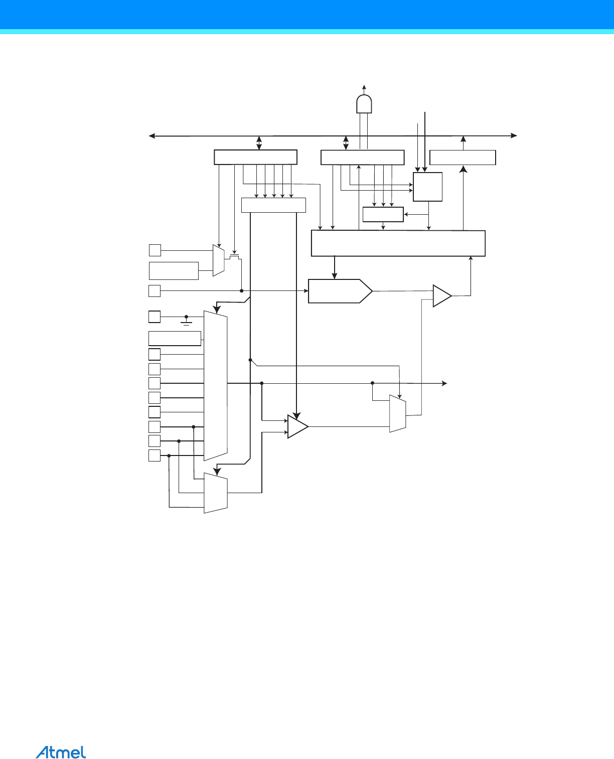
Figure 23-1. Analog to Digital Converter Block Schematic
23.3 Operation
The ADC converts an analog input voltage to a 10-bit digital value through successive approximation. The mini-
mum value represents GND and the maximum value represents the voltage on the AREF pin minus 1 LSB.
Optionally, AVCC or an internal 2.56V reference voltage may be connected to the AREF pin by writing to the
REFSn bits in the ADMUX Register. The internal voltage reference may thus be decoupled by an external capaci-
tor at the AREF pin to improve noise immunity.
The analog input channel and differential gain are selected by writing to the MUX bits in ADMUX. Any of the ADC
input pins, as well as GND and a fixed bandgap voltage reference, can be selected as single ended inputs to the
ADC. A selection of ADC input pins can be selected as positive and negative inputs to the differential gain
amplifier.
If differential channels are selected, the differential gain stage amplifies the voltage difference between the
selected input channel pair by the selected gain factor. This amplified value then becomes the analog input to the
ADC. If single ended channels are used, the gain amplifier is bypassed altogether.
ADC CONVERSION
COMPLETE IRQ
8-BIT DATA BUS
15 0
ADC MULTIPLEXER
SELECT (ADMUX)
ADC CTRL. & STATUS
REGISTER (ADCSRA)
ADC DATA REGISTER
(ADCH/ADCL)
MUX2
ADIE
ADATE
ADSC
ADEN
ADIF
ADIF
MUX1
MUX0
ADPS0
ADPS1
ADPS2
MUX3
CONVERSION LOGIC
10-BIT DAC
+
-
SAMPLE & HOLD
COMPARATOR
INTERNAL 2.56V
REFERENCE
MUX DECODER
MUX4
AVCC
ADC7
ADC6
ADC5
ADC4
ADC3
ADC2
ADC1
ADC0
REFS0
REFS1
ADLAR
+
-
CHANNEL SELECTION
GAIN SELECTION
ADC[9:0]
ADC MULTIPLEXER
OUTPUT
GAIN
AMPLIFIER
AREF
BANDGAP
REFERENCE
PRESCALER
SINGLE ENDED / DIFFERENTIAL SELECTION
GND
POS.
INPUT
MUX
NEG.
INPUT
MUX
TRIGGER
SELECT
ADTS[2:0]
INTERRUPT
FLAGS
START