
Instructions


ATmega328P Xplained Mini User Guide [USER GUIDE]
42287A-MCU-05/2014
12
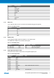
Table 2-11. Target uC I/O Signals not connected to any Connector or Header
ATmega328P pin Grid position
ADC6 H5
ADC7 G5
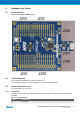
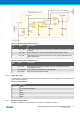
2.3.9 Extension headers
The marked area on the grid I7 to R8 can be used for strapping in a Xplained PRO extension header and a few
other headers based on the SPI bus.
The general bus connections for a Xplained PRO Extension board is indicated in the table below, detailed
wiring can be found in the selected Extension board documentation.
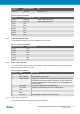
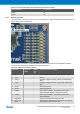
Table 2-12. Xplained Pro Extension Header
Pin Name Typical µC
signal
Typical
grid
pin
Extension signal description
1 ID NC Communication line to the ID chip on extension board.
2 GND Ground.
3 ADC(+) Analogue to digital converter, positive part of differential
ADC.
4 ADC(-) Analogue to digital converter, negative part of differential
ADC.
5 GPIO1 General purpose IO.
6 GPIO2 General purpose IO.
7 PWM(+) Pulse width modulation , alternatively positive part of
differential PWM. RESET to RF Extension board.
8 PWM(-) Pulse width modulation , alternatively positive part of
differential PWM.
9 IRQ/GPIO Interrupt request line from extension board.
10 SPI_SS_B/
GPIO
Slave select for SPI and/or general purpose I/O. Wake up
interrupt to RF extension (SLP_TR).