
Instructions

ATmega328P Xplained Mini User Guide [USER GUIDE]
42287A-MCU-05/2014
10
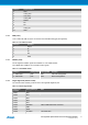
J200 pin &
location
ATmega328P pin Note
J200-10 PC5/SCL TWI Serial Clock.
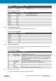
Table 2-5. J201 I/O Low Header
J201 pin ATmega328P pin Note
J201-1 PD0/RxD Target USART Receive Pin.
J201-2 PD1/TxD Target USART Transmit Pin.
J201-3 PD2
J201-4 PD3
J201-5 PD4
J201-6 PD5
J201-7 PD6
J201-8 PD7
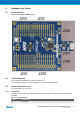
2.3.5 Target Analogue I/O (J203)
The ATmega328P analogue I/O pins are available in the J203 header.
Table 2-6. J200 Analogue Header
J203 pin & location ATmega328P pin
J203-1 PC0
J203-2 PC1
J203-3 PC2
J203-4 PC3
J203-5 PC4
J203-6 PC5
2.3.6 Power (J202, J300, J301)
The J300 and J301 headers enables selection of power sources and target supply power, the J202 header
enables connection to the power system.
Table 2-7. J202 Power Header
J202 pin Signal Description
1 NC.
2 VCC_TARGET ATmega328P supply voltage.
3 RESET_SENSE RESET from external source, monitored by the mEDBG, if pulled low the
target RESET line will be pulled low. Possible to connect directly to the
target by assembling R212 and removing R110. Note: DebgWIRE will
then be disabled.
4 VCC_P3V3 3.3V from on-board DC/DC converter (U300).
5 VCC_P5V0 Voltage from the selected power source, default VBUS.
6 GND
7 GND
8 VCC_VIN The externally connected power source if any.
2.3.6.1 Power supply configuration
The J300 and J301 headers enables Power supply configuration.