USER GUIDE ATmega328P Xplained Mini User Guide Introduction ® This user guide describes how to get started with the Atmel ATmega328P Xplained Mini board. The ATmega328P Xplained Mini evalutation kit is a hardware platform to evaluate the Atmel ATmega328P microcontroller. The evaluation kit comes with a fully integrated debugger that provides seamless integration with Atmel Studio 6.2 (and later version).
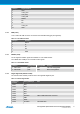
Table of Contents Introduction .................................................................................... 1 1. Getting Started ........................................................................ 3 1.1. 1.2. 1.3. 1.4. 1.5. 1.6. Features .............................................................................. Design Documentation and Related Links .................................. Board Assembly .................................................................... 1.3.1.
1. Getting Started 1.1 Features The ATmega328P Xplained Mini evaluation board provides a development platform for the Atmel ATmega328P. 1.2 Design Documentation and Related Links The most relevant documents and software for the evaluation board is available here: http://www.atmel.com/tools/XplainedMini.aspx 1.3 Board Assembly The Xplained Mini board is very flexible and can be used in a number of ways. E.g. as your own prototype for SW development and HW verification. 1.3.
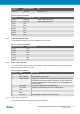
1.5 Programming and Debugging How to program and debug the Xplained Mini board. 1.5.1 Programming the Target Using mEDBG Using the Embedded Debugger on the Xplained Mini board to program the ATmega328 via the SPI bus. 1. Connect the mEDBG USB to the PC. 2. Go to Atmel Studio: click Tools, select Device Programming, and select the connected mEDBG as Tool with Device = ATmega328P and Interface = ISP, click Apply. Note that if ISP programming fails it could be because debugWIRE is enabled.
Important 1.5.3 If any other cpu clk than the external clk supplied by the mEDBG is used the debugWIRE is not guaranteed to work. Programming the Target Using an External Programmer ® How to program the target ATmega328P using the AVR JTAGICE mkII, JTAGICE3, or other Atmel Programmers. 1. Connect the External Programmer to the PC. 2. Connect the External Programme to the evaluation board ISP connector (J204) (Need the 6-pin 100mil adapter connected to the JTAGICE). 3.
BOOTRST = [ ] CKDIV8 = [ ] CKOUT = [X] SUT_CKSEL = EXTXOSC_8MHZ_XX_258CK_65MS Important 1.5.5 CKOUT must be enabled the provide clock to the target. Programming the ATmega32U4 Using a Bootloader This section describes how to use the bootloader to program the ATmega32U4. 1. Install the Bootloader interface on the PC as described in “How to Install the "Bootloader PC tool"” on page 6. 2. Start the Bootloader PC GUI "FLIP". 3. Short strap J102. 4. Connect the board USB connector to the PC. 5.
2. 1.6 Run the Flip Installer. Available Example Code The ATmega328P is preprogrammed with a demo program, ReMorse. Source code is available in Atmel 3 Spaces . When the CDC COM port is connected to a terminal window, the text you write will be transmitted via the LED in Morse code. Any Morse code transmitted by using the switch will be displayed as text in the terminal window. 3 http://spaces.atmel.
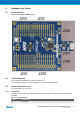
2. Hardware User Guide 2.1 Board Overview Figure 2-1. ATmega328P-XMINI Overview 2.2 Clock Distribution The ATmega32U4 (mEDBG) has an external 16MHz XTAL. The ATmega32U4 provides an external 16MHz clock to the ATmega328P (target). 2.3 Headers and Connectors The board headers and connectors. 2.3.1 JTAG (J100) J100 is the JTAG programming header typically used by the JTAGICE for programming of the ATmega32U4 (mEDBG). Table 2-1.
2.3.2 J100 pin Signal function 2 GND 3 JTAG_TDO 4 VCC (5V0) 5 JTAG_TMS 6 RESET 7 NC 8 NC 9 JTAG_TDI 10 GND USB (J101) J101 is a Micro-B USB connector connected to the embedded debugger (ATmega32U4). Table 2-2. J101 USB Connector 2.3.3 J101 pin Function 1 VBUS 2 D- 3 D+ 4 NC 5 GND USART (J104) The ATmega32U4 USART signals are available on J104 USART header. The mEDBG CDC COM port is connected to these signals. Table 2-3. J104 USART Header 2.3.
J200 pin & location ATmega328P pin Note J200-10 PC5/SCL TWI Serial Clock. Table 2-5. J201 I/O Low Header 2.3.5 J201 pin ATmega328P pin Note J201-1 PD0/RxD Target USART Receive Pin. J201-2 PD1/TxD Target USART Transmit Pin. J201-3 PD2 J201-4 PD3 J201-5 PD4 J201-6 PD5 J201-7 PD6 J201-8 PD7 Target Analogue I/O (J203) The ATmega328P analogue I/O pins are available in the J203 header. Table 2-6. J200 Analogue Header 2.3.
Table 2-8. J300 Board External Power Selection J300 pin Signal Description 1 VCC_VBUS VBUS Pin of USB Connector via fuse F100, by default connected to VCC_P5V0 via R300. 2 VCC_P5V0 Input voltage (4.3 to 16V) for the fixed-output voltage regulator (U300). 3 VCC_VIN Alternative power source for the board (4.3 to 16V), study U300 data sheet for detail requirements. Table 2-9. J301 Board Power Supply Selection 2.3.
Table 2-11. Target uC I/O Signals not connected to any Connector or Header 2.3.9 ATmega328P pin Grid position ADC6 H5 ADC7 G5 Extension headers The marked area on the grid I7 to R8 can be used for strapping in a Xplained PRO extension header and a few other headers based on the SPI bus. The general bus connections for a Xplained PRO Extension board is indicated in the table below, detailed wiring can be found in the selected Extension board documentation. Table 2-12.
Pin Name Typical µC signal Typical grid pin Extension signal description 11 TWI_SDA PC4/SDA M6 to Q12 Data line for two wire interface. 12 TWI_SCL PC5/SCL M9 to R12 Clock line for two wire interface. 13 USART_RX PD0/RXD L6 to A12 USART Input Pin from extension board, remove R107 if used. 14 USART_TX PD1/TXD L9 to B12 USART Output Pin to extension board, remove R108 if used. 15 SPI_SS_A PB2/SS K6 to K5.5 Slave select for Serial peripheral interface.
Table 2-14. Button 2.5 Button Function ATmega328P pin SW200 User defined high signal, press to ground (negate). 8 - PB7 Factory Programmed Data The ATmega328P Xplained Mini board comes with a demo program preprogrammed in the ATmega328P FLASH using the external clock provided by the ATmega32U4. The ATmega32U4 is preprogrammed with the mEDBG. 2.6 Errata The following should be noted on revision 2 of the board ( A09-2323/2): 1.
3.
Atmel Corporation 1600 Technology Drive, San Jose, CA 95110 USA T: (+1)(408) 441.0311 F: (+1)(408) 436.4200 | www.atmel.com © 2014 Atmel Corporation. All rights reserved. / Rev.: 42287A-MCU-05/2014 ® ® ® Atmel , Atmel logo and combinations thereof, Enabling Unlimited Possibilities , AVR , and others are registered trademarks or trademarks of Atmel Corporation or its subsidiaries. Other terms and product names may be trademarks of others.