
Data Sheet

90
ATmega48A/PA/88A/PA/168A/PA/328/P [DATASHEET]
Atmel-8271H-AVR- ATmega-Datasheet_08/2014
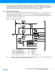
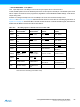
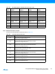
The alternate pin configuration is as follows:
• AIN1/OC2B/PCINT23 – Port D, Bit 7
AIN1, Analog Comparator Negative Input. Configure the port pin as input with the internal pull-up switched off to
avoid the digital port function from interfering with the function of the Analog Comparator.
PCINT23: Pin Change Interrupt source 23. The PD7 pin can serve as an external interrupt source.
• AIN0/OC0A/PCINT22 – Port D, Bit 6
AIN0, Analog Comparator Positive Input. Configure the port pin as input with the internal pull-up switched off to
avoid the digital port function from interfering with the function of the Analog Comparator.
OC0A, Output Compare Match output: The PD6 pin can serve as an external output for the Timer/Counter0
Compare Match A. The PD6 pin has to be configured as an output (DDD6 set (one)) to serve this function. The
OC0A pin is also the output pin for the PWM mode timer function.
PCINT22: Pin Change Interrupt source 22. The PD6 pin can serve as an external interrupt source.
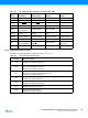
• T1/OC0B/PCINT21 – Port D, Bit 5
T1, Timer/Counter1 counter source.
OC0B, Output Compare Match output: The PD5 pin can serve as an external output for the Timer/Counter0
Compare Match B. The PD5 pin has to be configured as an output (DDD5 set (one)) to serve this function. The
OC0B pin is also the output pin for the PWM mode timer function.
PCINT21: Pin Change Interrupt source 21. The PD5 pin can serve as an external interrupt source.
• XCK/T0/PCINT20 – Port D, Bit 4
XCK, USART external clock.
T0, Timer/Counter0 counter source.
PCINT20: Pin Change Interrupt source 20. The PD4 pin can serve as an external interrupt source.
• INT1/OC2B/PCINT19 – Port D, Bit 3
INT1, External Interrupt source 1: The PD3 pin can serve as an external interrupt source.
OC2B, Output Compare Match output: The PD3 pin can serve as an external output for the Timer/Counter0
Compare Match B. The PD3 pin has to be configured as an output (DDD3 set (one)) to serve this function. The
OC2B pin is also the output pin for the PWM mode timer function.
PCINT19: Pin Change Interrupt source 19. The PD3 pin can serve as an external interrupt source.
• INT0/PCINT18 – Port D, Bit 2
INT0, External Interrupt source 0: The PD2 pin can serve as an external interrupt source.
PCINT18: Pin Change Interrupt source 18. The PD2 pin can serve as an external interrupt source.
• TXD/PCINT17 – Port D, Bit 1
TXD, Transmit Data (Data output pin for the USART). When the USART Transmitter is enabled, this pin is
configured as an output regardless of the value of DDD1.
PCINT17: Pin Change Interrupt source 17. The PD1 pin can serve as an external interrupt source.